SLES142B JUNE 2005 – July 2016 PCM1803A
PRODUCTION DATA.
- 1 Features
- 2 Applications
- 3 Description
- 4 Revision History
- 5 Pin Configuration and Functions
- 6 Specifications
- 7 Detailed Description
- 8 Application and Implementation
- 9 Power Supply Recommendations
- 10Layout
- 11Device and Documentation Support
- 12Mechanical, Packaging, and Orderable Information
7 Detailed Description
7.1 Overview
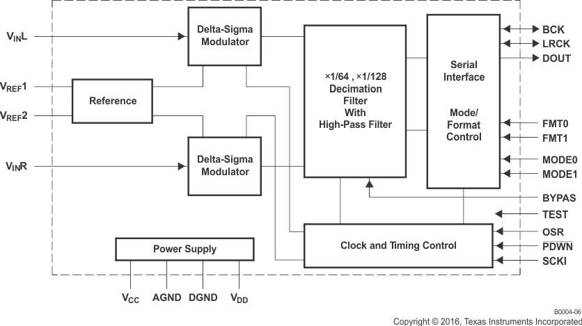
The PCM1803A is suitable for a wide variety of cost-sensitive consumer applications where good performance and operation from a 5-V analog supply and 3.3-V digital supply are required. With hardware control and straightforward operation, the PCM1803A can quickly be implemented into an application. The PCM1803A supports sampling rates from 16 kHz to 96 kHz as well as left justified, right justified, and I2S formats, allowing its use in a variety of audio systems.
7.2 Functional Block Diagram
7.3 Feature Description
7.3.1 Hardware Control
Pins FMT0, FMT1, OSR, BYPASS, MD0, and MD1 allow the device to be controlled by either tying these pins to GND, or VDD, as well as GPIO, from a host IC. These controls allow full configuration of the PCM1803A.
7.3.2 Power-On-Reset Sequence
The PCM1803A has an internal power-on-reset circuit, and initialization (reset) is performed automatically at the time when power-supply voltage (VDD) exceeds 2.2 V (typical). While VDD < 2.2 V (typical) and for 1024 system clock cycles after VDD > 2.2 V (typical), the PCM1803A stays in the reset state, and the digital output is forced to zero. The digital output becomes valid when a time period of 4480/fS has elapsed following release from the reset state. Figure 17 illustrates the internal power-on-reset timing and the digital output for power-on reset.
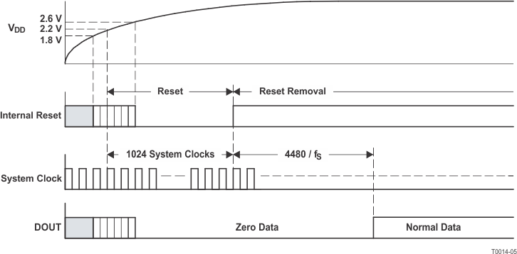 Figure 17. Internal Power-On-Reset Timing
7.3.3 System Clock
The PCM1803A supports 256 fS, 384 fS, 512 fS, and 768 fS as the system clock, where fS is the audio sampling frequency. The system clock must be supplied on SCKI (pin 15).
The PCM1803A has a system clock-detection circuit that automatically senses if the system clock is operating at 256 fS, 384 fS, 512 fS, or 768 fS in slave mode. In master mode, the system clock frequency must be selected by MODE0 (pin 19) and MODE1 (pin 20), and 768 fS is not available. The system clock is divided automatically into 128 fS and 64 fS, and these frequencies are used to operate the digital filter and the delta-sigma modulator.
Table 1 shows the relationship of typical sampling frequency and system clock frequency, and Figure 18 shows system clock timing.
Table 1. Sampling Frequency and System Clock Frequency
| SAMPLING FREQUENCY (kHz) | SYSTEM CLOCK FREQUENCY (MHz) | |||
|---|---|---|---|---|
| 256 fS | 384 fS | 512 fS | 768 fS (1) | |
| 32 | 8.1920 | 12.2880 | 16.3840 | 24.5760 |
| 44.1 | 11.2896 | 16.9344 | 22.5792 | 33.8688 |
| 48 | 12.2880 | 18.4320 | 24.5760 | 36.8640 |
| 64 | 16.3840 | 24.5760 | 32.7680 | 49.1520 |
| 88.2 | 22.5792 | 33.8688 | 45.1584 | – |
| 96 | 24.5760 | 36.8640 | 49.1520 | – |
 Figure 18. System Clock Timing
Table 2. System Clock Timing Requirements
| PARAMETER | MIN | MAX | UNIT | |
|---|---|---|---|---|
| tw(SCKH) | System clock pulse duration, HIGH | 8 | ns | |
| tw(SCKL) | System clock pulse duration, LOW | 8 | ns | |
The quality of the system clock can influence the dynamic performance, because the PCM1803A operates based on a system clock. Therefore, it may be required to consider the system-clock duty, jitter, and the time difference between system-clock transition and BCK or LRCK transition in the slave mode.
7.4 Device Functional Modes
7.4.1 Serial Audio Data Interface
The PCM1803A interfaces the audio system through BCK (pin 11), LRCK (pin 10), and DOUT (pin 12).
7.4.1.1 Interface Mode
The PCM1803A supports master mode and slave mode as interface modes, and they are selected by MODE1 (pin 20) and MODE0 (pin 19) as shown in Table 3.
In master mode, the PCM1803A provides the timing of serial audio data communications between the PCM1803A and the digital audio processor or external circuit. While in slave mode, the PCM1803A receives the timing for data transfers from an external controller.
Table 3. Interface Mode
| MODE1 | MODE0 | INTERFACE MODE |
|---|---|---|
| 0 | 0 | Slave mode (256 fS, 384 fS, 512 fS, 768 fS) |
| 0 | 1 | Master mode (512 fS) |
| 1 | 0 | Master mode (384 fS) |
| 1 | 1 | Master mode (256 fS) |
7.4.1.1.1 Master Mode
In master mode, BCK and LRCK work as output pins, and these pins are controlled by timing, which is generated in the clock circuit of the PCM1803A. The frequency of BCK is fixed at LRCK × 64. The 768-fS system clock is not available in master mode.
7.4.1.1.2 Slave Mode
In slave mode, BCK and LRCK work as input pins. The PCM1803A accepts the 64-BCK/LRCK or 48-BCK/LRCK format (only for 384 fS and 768 fS system clocks), not the 32-BCK/LRCK format.
7.4.1.2 Data Format
The PCM1803A supports four audio data formats in both master and slave modes, and the data formats are selected by FMT1 (pin 18) and FMT0 (pin 17) as shown in Table 4. Figure 19 illustrates the data formats in slave and master modes.
Table 4. Data Formats
| FORMAT | FMT1 | FMT0 | DESCRIPTION |
|---|---|---|---|
| 0 | 0 | 0 | Left-justified, 24-bit |
| 1 | 0 | 1 | I2S, 24-bit |
| 2 | 1 | 0 | Right-justified, 24-bit |
| 3 | 1 | 1 | Right-justified, 20-bit |
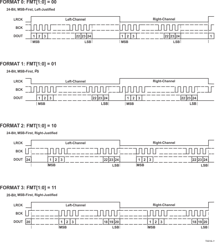 Figure 19. Audio Data Formats (LRCK and BCK Work as Inputs in Slave Mode and as Outputs in Master Mode)
7.4.1.3 Interface Timing
Figure 20 illustrates the interface timing in slave mode; Figure 21 and Figure 22 illustrate the interface timing in master mode.
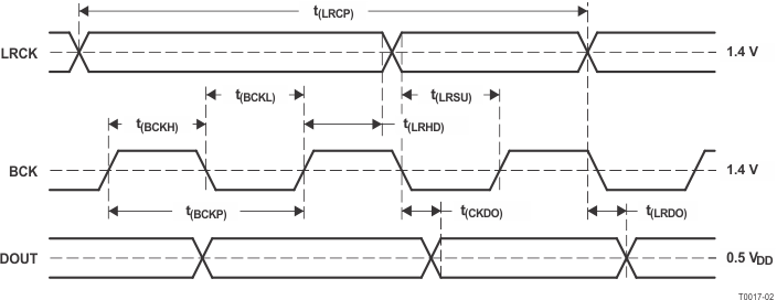 Figure 20. Audio Data Interface Timing (Slave Mode: LRCK and BCK Work as Inputs)
Table 5. Audio Data Interface Slave Mode Timing Requirements(1)
| PARAMETER | MIN | TYP | MAX | UNIT | |
|---|---|---|---|---|---|
| t(BCKP) | BCK period | 1/(64 fS) | ns | ||
| t(BCKH) | BCK pulse duration, HIGH | 1.5 × t(SCKI) | ns | ||
| t(BCKL) | BCK pulse duration, LOW | 1.5 × t(SCKI) | ns | ||
| t(LRSU) | LRCK setup time to BCK rising edge | 40 | ns | ||
| t(LRHD) | LRCK hold time to BCK rising edge | 20 | ns | ||
| t(LRCP) | LRCK period | 10 | μs | ||
| t(CKDO) | Delay time, BCK falling edge to DOUT valid | –10 | 40 | ns | |
| t(LRDO) | Delay time, LRCK edge to DOUT valid | –10 | 40 | ns | |
| tr | Rising time of all signals | 20 | ns | ||
| tf | Falling time of all signals | 20 | ns | ||
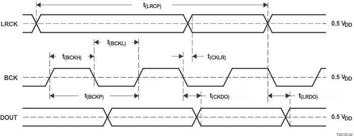 Figure 21. Audio Data Interface Timing (Master Mode: LRCK and BCK Work as Outputs)
Table 6. Audio Data Interface Master Mode Timing Requirements(1)
| PARAMETER | MIN | TYP | MAX | UNIT | |
|---|---|---|---|---|---|
| t(BCKP) | BCK period | 150 | 1/(64 fS) | 1000 | ns |
| t(BCKH) | BCK pulse duration, HIGH | 65 | 600 | ns | |
| t(BCKL) | BCK pulse duration, LOW | 65 | 600 | ns | |
| t(CKLR) | Delay time, BCK falling edge to LRCK valid | –10 | 20 | ns | |
| t(LRCP) | LRCK period | 10 | 1/fS | 65 | μs |
| t(CKDO) | Delay time, BCK falling edge to DOUT valid | –10 | 20 | ns | |
| t(LRDO) | Delay time, LRCK edge to DOUT valid | –10 | 20 | ns | |
| tr | Rising time of all signals | 20 | ns | ||
| tf | Falling time of all signals | 20 | ns | ||
 Figure 22. Audio Clock Interface Timing (Master Mode: BCK Works as Output)
Table 7. Audio Data Interface Master Mode BCK Timing Requirements(1)
| PARAMETER | MIN | TYP | MAX | UNIT | |
|---|---|---|---|---|---|
| t(SCKBCK) | Delay time, SCKI rising edge to BCK edge | 5 | 30 | ns | |
7.4.2 Synchronization With Digital Audio System
In slave mode, the PCM1803A operates under LRCK, synchronized with system clock SCKI. The PCM1803A does not need a specific phase relationship between LRCK and SCKI, but does require the synchronization of LRCK and SCKI.
If the relationship between LRCK and SCKI changes more than ±6 BCKs for 64 BCK/frame (±5 BCKs for 48 BCK/frame) during one sample period due to LRCK or SCKI jitter, internal operation of the ADC halts within 1/fS, and digital output is forced to zero data (BPZ code) until resynchronization between LRCK and SCKI occurs.
In case of changes less than ±5 BCKs for 64 BCK/frame (±4 BCKs for 48 BCK/frame), resynchronization does not occur and the previously explained digital output control and discontinuity do not occur.
Figure 23 illustrates the digital output response for loss of synchronization and resynchronization. During undefined data, the PCM1803A can generate some noise in the audio signal. Also, the transition of normal to undefined data and undefined or zero data to normal creates a discontinuity in the data of the digital output, which can generate some noise in the audio signal.
 Figure 23. ADC Digital Output for Loss of Synchronization and Resynchronization
7.4.3 Power Down
PDWN (pin 7) controls operation of the entire ADC. During power-down mode, supply current for the analog portion is shut down and the digital portion is reset; also, DOUT (pin 12) is disabled. It is acceptable to halt the system clock during power-down mode so that power dissipation is minimized. The minimum LOW pulse duration on the PDWN pin is 100 ns.
TI recommends setting PWDN (pin 7) to LOW once to obtain stable analog performance when the sampling rate, interface mode, data format, or oversampling control is changed.
Table 8. Power-Down Control
| PWDN | POWER-DOWN MODE |
|---|---|
| LOW | Power-down mode |
| HIGH | Normal operation mode |
7.4.4 HPF Bypass
The built-in function for DC-component rejection can be bypassed by BYPAS (pin 8) control. In bypass mode, the DC component of the input analog signal, internal DC offset, and so forth, also are converted and included in the digital output data.
Table 9. HPF Bypass Control
| BYPAS | HPF (HIGH-PASS FILTER) MODE |
|---|---|
| LOW | Normal (no DC component in DOUT) mode |
| HIGH | Bypass (DC component in DOUT) mode |
7.4.5 Oversampling Ratio Control
OSR (pin 16) controls the oversampling ratio of the delta-sigma modulator, ×64 or ×128. The ×128 mode is available for fS ≤ 48 kHz.
Table 10. Oversampling Control
| OSR | OVERSAMPLING RATIO |
|---|---|
| LOW | ×64 |
| HIGH | ×128 (fS ≤ 48 kHz) |