SLES023D December 2001 – December 2016 PCM1802
PRODUCTION DATA.
- 1 Features
- 2 Applications
- 3 Description
- 4 Revision History
- 5 Pin Configuration and Functions
-
6 Specifications
- 6.1 Absolute Maximum Ratings
- 6.2 ESD Ratings
- 6.3 Recommended Operating Conditions
- 6.4 Thermal Information
- 6.5 Electrical Characteristics
- 6.6 Typical Characteristics
- 7 Detailed Description
- 8 Application and Implementation
- 9 Power Supply Recommendations
- 10Layout
- 11Device and Documentation Support
- 12Mechanical, Packaging, and Orderable Information
6 Specifications
6.1 Absolute Maximum Ratings
over operating free-air temperature range (unless otherwise noted)(1)| MIN | MAX | UNIT | ||
|---|---|---|---|---|
| Supply voltage | VCC | 6.5 | V | |
| VDD | 4 | |||
| Ground voltage differences | AGND and DGND | ±0.1 | V | |
| Supply voltage difference (VCC – VDD) | VCC and VDD | 3 V | V | |
| Digital input voltage | FSYNC, LRCK, BCK, and DOUT | –0.3 | VDD + 0.3 | V |
| PDWN, BYPAS, SCKI, OSR, FMT0, FMT1, MODE0, and MODE1 | –0.3 | 6.5 | ||
| Analog input voltage | VINL, VINR, VREF1, and VREF2 | –0.3 | VCC + 0.3 | V |
| Input current (any pins except supplies) | ±10 | mA | ||
| Ambient temperature under bias | –40 | 125 | °C | |
| Junction temperature | 150 | °C | ||
| Package temperature (IR reflow, peak) | 260 | °C | ||
| Storage temperature, Tstg | –55 | 150 | °C | |
6.2 ESD Ratings
| VALUE | UNIT | |||
|---|---|---|---|---|
| V(ESD) | Electrostatic discharge | Human-body model (HBM), per ANSI/ESDA/JEDEC JS-001(1) | ±1500 | V |
| Charged-device model (CDM), per JEDEC specification JESD22-C101(2) | ±1000 | |||
6.3 Recommended Operating Conditions
over operating free-air temperature range (unless otherwise noted)| MIN | NOM | MAX | UNIT | ||
|---|---|---|---|---|---|
| Analog supply voltage, VCC | 5 | V | |||
| Digital supply voltage, VDD | 3.3 | V | |||
| Analog input voltage, full-scale (–0 dB) | 3 | VP–P | |||
| Digital input logic family | TTL | ||||
| Digital input clock frequency | Sampling clock | 8.192 | 49.152 | MHz | |
| System clock | 32 | 96 | kHz | ||
| Digital output load capacitance | 20 | pF | |||
| Operating free-air temperature, TA | –40 | 85 | °C | ||
6.4 Thermal Information
| THERMAL METRIC(1) | PCM1802 | UNIT | |
|---|---|---|---|
| DB (SSOP) | |||
| 20 PINS | |||
| RθJA | Junction-to-ambient thermal resistance | 80.8 | °C/W |
| RθJC(top) | Junction-to-case (top) thermal resistance | 40 | °C/W |
| RθJB | Junction-to-board thermal resistance | 37.6 | °C/W |
| ψJT | Junction-to-top characterization parameter | 7.2 | °C/W |
| ψJB | Junction-to-board characterization parameter | 37 | °C/W |
6.5 Electrical Characteristics
TA = 25°C, VCC = 5 V, VDD = 3.3 V, master mode, fS = 44.1 kHz, system clock = 384 fS, oversampling ratio = ×128, 24-bit data (unless otherwise noted)| PARAMETER | TEST CONDITIONS | MIN | TYP | MAX | UNIT | ||
|---|---|---|---|---|---|---|---|
| Resolution | 24 | Bits | |||||
| DATA FORMAT | |||||||
| Audio data interface format | Left-justified, I2S, or right‑justified | ||||||
| Audio data bit length | 20 or 24 | Bits | |||||
| Audio data format | MSB first or 2s complement | ||||||
| fS | Sampling frequency | 16 | 44.1 | 96 | kHz | ||
| System clock frequency | 256 fS | 4.096 | 11.2896 | 24.576 | MHz | ||
| 384 fS | 6.144 | 16.9344 | 36.864 | ||||
| 512 fS | 8.192 | 22.5792 | 49.152 | ||||
| 768 fS(1) | 12.288 | 33.8688 | |||||
| INPUT LOGIC | |||||||
| VIH | Input logic level(2) | 2 | VDD | VDC | |||
| VIL | 0 | 0.8 | |||||
| VIH | Input logic level(3) | 2 | 5.5 | ||||
| VIL | 0 | 0.8 | |||||
| IIH | Input logic current(4) | VIN = VDD | ±10 | µA | |||
| IIL | VIN = 0 V | ±10 | |||||
| IIH | Input logic current(5) | VIN = VDD | 65 | 100 | |||
| IIL | VIN = 0 V | ±10 | |||||
| OUTPUT LOGIC | |||||||
| VOH | Output logic level(6) | IOUT = –1 mA | 2.8 | VDC | |||
| VOL | IOUT = 1 mA | 0.5 | |||||
| DC ACCURACY | |||||||
| Gain mismatch, channel-to-channel |
±1% | ±4% | FSR | ||||
| Gain error | ±2% | ±6% | FSR | ||||
| Bipolar zero error | HPF bypassed(7) | ±2% | FSR | ||||
| DYNAMIC PERFORMANCE(8) | |||||||
| THD+N | Total harmonic distortion + noise | fS = 44.1 kHz, VIN = –0.5 dB | 0.0015% | 0.003% | |||
| fS = 96 kHz, VIN = –0.5 dB, system clock = 256 fS, oversampling ratio = ×64(9) | 0.0025% | ||||||
| fS = 44.1 kHz, VIN = –60 dB | 0.7% | ||||||
| fS = 96 kHz, VIN = –60 dB, system clock = 256 fS, oversampling ratio = ×64(9) | 1.2% | ||||||
| Dynamic range | fS = 44.1 kHz, A-weighted | 100 | 105 | dB | |||
| fS = 96 kHz, A-weighted, system clock = 256 fS, oversampling ratio = ×64(9) | 103 | ||||||
| Signal to noise ratio | fS = 44.1 kHz, A-weighted | 100 | 105 | dB | |||
| fS = 96 kHz, A-weighted, system clock = 256 fS, oversampling ratio = ×64(9) | 103 | ||||||
| Channel separation | fS = 44.1 kHz | 96 | 103 | dB | |||
| fS = 96 kHz, system clock = 256 fS, oversampling ratio = ×64(9) | 98 | ||||||
| ANALOG INPUT | |||||||
| Input voltage | 0.6 × VCC | VP–P | |||||
| VREF1 | Center voltage | 0.5 × VCC | V | ||||
| Input impedance | 20 | kΩ | |||||
| Antialiasing filter frequency response | –3 dB | 300 | kHz | ||||
| DIGITAL FILTER PERFORMANCE | |||||||
| Pass band | 0.454 fS | Hz | |||||
| Stop band | 0.583 fS | Hz | |||||
| Pass-band ripple | ±0.05 | dB | |||||
| Stop-band attenuation | –65 | dB | |||||
| Delay time | 17.4 / fS | s | |||||
| HPF frequency response | –3 dB | 0.019 fS | mHz | ||||
| POWER SUPPLY REQUIREMENTS | |||||||
| VCC | Voltage | 4.5 | 5 | 5.5 | VDC | ||
| VDD | 2.7 | 3.3 | 3.6 | ||||
| ICC | Supply current(10) | VCC = 5 V, VDD = 3.3 V | 24 | 30 | mA | ||
| IDD | fS = 44.1 kHz VCC = 5 V, VDD = 3.3 V | 8.3 | 10 | ||||
| fS = 96 kHz, VCC = 5 V, VDD = 3.3 V(8) | 17 | ||||||
| PD | Power dissipation | Operation | fS = 44.1 kHz, VCC = 5 V, VDD = 3.3 V | 147 | 183 | mW | |
| fS = 96 kHz, VCC = 5 V, VDD = 3.3 V(8) | 176 | ||||||
| Power down | VCC = 5 V, VDD = 3.3 V | 0.5 | |||||
6.6 Typical Characteristics
TA = 25°C, VCC = 5 V, VDD = 3.3 V, Master mode, fS = 44.1 kHz, system clock = 384 fS, oversampling ratio = ×128, and 24-bit data (unless otherwise noted).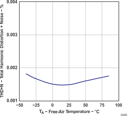 Figure 1. Total Harmonic Distortion + Noise
 vs Free-Air Temperature
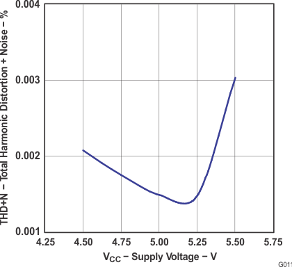 Figure 3. Total Harmonic Distortion + Noise
 vs Supply Voltage
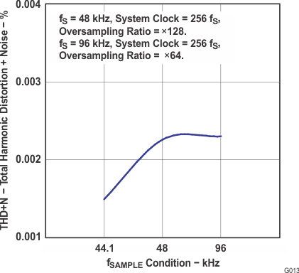 Figure 5. Total Harmonic Distortion + Noise
 vs fSAMPLE Condition
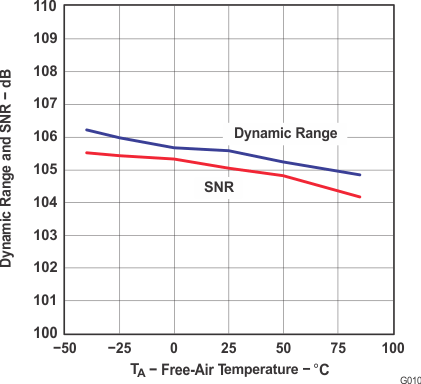 Figure 2. Dynamic Range and SNR
vs Free-Air Temperature
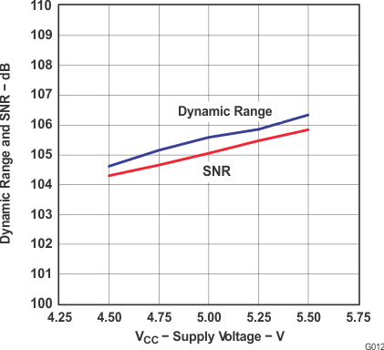 Figure 4. Dynamic Range and SNR vs Suppy Voltage
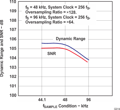 Figure 6. Dynamic Range and SNR vs fSAMPLE Condition
6.6.1 Typical Characteristics: Internal Filter
6.6.1.1 Digital Filter: Decimation Filter Frequency Response
TA = 25°C, VCC = 5 V, VDD = 3.3 V, Master mode, fS = 44.1 kHz, system clock = 384 fS, oversampling ratio = ×128, and 24-bit data (unless otherwise noted).
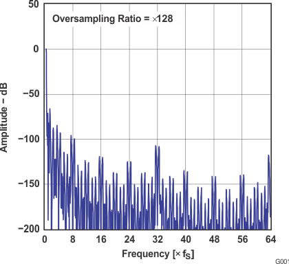 Figure 7. Amplitude vs Frequency Overall Characteristics
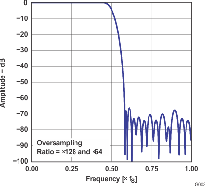 Figure 9. Amplitude vs Frequency Stop-Band Attenuation Characteristics
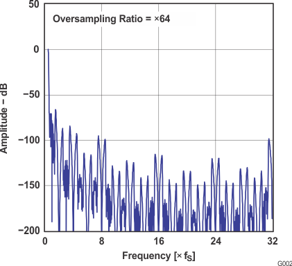 Figure 8. Amplitude vs Frequency Overall Characteristics
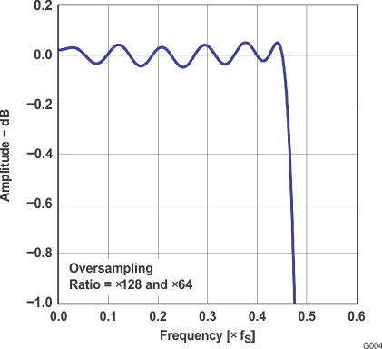 Figure 10. Amplitude vs Frequency Pass-Band Ripple Characteristics
6.6.1.2 HPF (High-Pass Filter) Frequency Response
TA = 25°C, VCC = 5 V, VDD = 3.3 V, Master mode, fS = 44.1 kHz, system clock = 384 fS, oversampling ratio = ×128, and 24-bit data (unless otherwise noted).
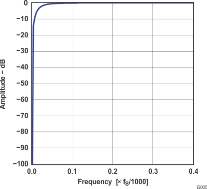 Figure 11. Amplitude vs Frequency HPF
Stop-Band Characteristics
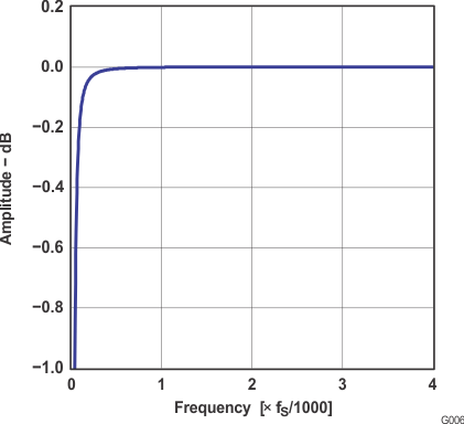 Figure 12. Amplitude vs Frequency HPF
Pass-Band Characteristics
6.6.1.3 Analog Filter: Antialiasing Filter Frequence Response
TA = 25°C, VCC = 5 V, VDD = 3.3 V, Master mode, fS = 44.1 kHz, system clock = 384 fS, oversampling ratio = ×128, and 24-bit data (unless otherwise noted).
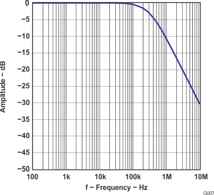 Figure 13. Amplitude vs Frequency Antialias Filter Stop-Band Characteristics
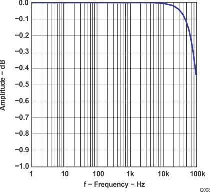 Figure 14. Amplitude vs Frequency Antialias Filter Pass-Band Characteristics
6.6.2 Typical Characteristics: Output Spectrum
TA = 25°C, VCC = 5 V, VDD = 3.3 V, Master mode, fS = 44.1 kHz, system clock = 384 fS, oversampling ratio = ×128, and 24-bit data (unless otherwise noted).
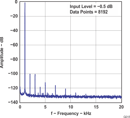 Figure 15. Amplitude vs Frequency
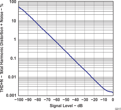 Figure 17. Total Harmonic Distortion + Noise vs Signal Level
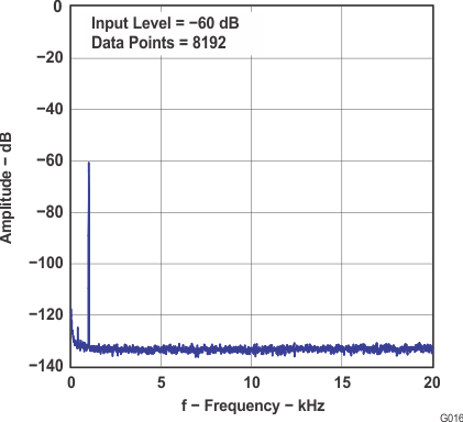 Figure 16. Amplitude vs Frequency
6.6.3 Typical Characteristics: Supply Current
TA = 25°C, VCC = 5 V, VDD = 3.3 V, Master mode, fS = 44.1 kHz, system clock = 384 fS, oversampling ratio = ×128, and 24-bit data (unless otherwise noted).
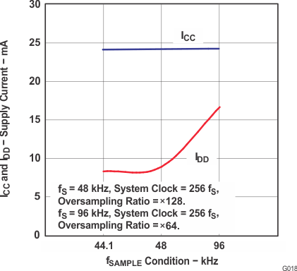 Figure 18. Supply Current vs fSAMPLE Condition