ZHCSEE9B August   2004  – December 2015 PCM1794A

PRODUCTION DATA.  

  1. 特性
  2. 应用
  3. 说明
  4. 修订历史记录
  5. Pin Configuration and Functions
  6. Specifications
    1. 6.1 Absolute Maximum Ratings
    2. 6.2 ESD Ratings
    3. 6.3 Recommended Operating Conditions
    4. 6.4 Thermal Information
    5. 6.5 Electrical Characteristics
    6. 6.6 Timing Requirements
    7. 6.7 Typical Characteristics
  7. Detailed Description
    1. 7.1 Overview
    2. 7.2 Functional Block Diagram
    3. 7.3 Feature Description
      1. 7.3.1 System Clock Input
      2. 7.3.2 Power-On and External Reset Functions
      3. 7.3.3 Audio Data Interface
        1. 7.3.3.1 Audio Serial Interface
        2. 7.3.3.2 PCM Audio Data Formats and Timing
      4. 7.3.4 Audio Data Format
      5. 7.3.5 Soft Mute
      6. 7.3.6 De-Emphasis
      7. 7.3.7 Zero Detect
      8. 7.3.8 Advanced Segment DAC
      9. 7.3.9 Analog Output
    4. 7.4 Device Functional Modes
      1. 7.4.1 Device Control
      2. 7.4.2 Audio Input Modes
      3. 7.4.3 Audio Output Modes
  8. Application and Implementation
    1. 8.1 Application Information
      1. 8.1.1 I/V Section
      2. 8.1.2 Differential Section
      3. 8.1.3 Interfacing With an External Digital Filter
        1. 8.1.3.1 System Clock (SCK) and Interface Timing
        2. 8.1.3.2 Audio Format
    2. 8.2 Typical Application
      1. 8.2.1 Design Requirements
      2. 8.2.2 Detailed Design Procedure
        1. 8.2.2.1 Audio Input or Output
      3. 8.2.3 Application Curves
  9. Power Supply Recommendations
  10. 10Layout
    1. 10.1 Layout Guidelines
    2. 10.2 Layout Example
  11. 11器件和文档支持
    1. 11.1 文档支持
      1. 11.1.1 相关文档 
    2. 11.2 社区资源
    3. 11.3 商标
    4. 11.4 静电放电警告
    5. 11.5 Glossary
  12. 12机械、封装和可订购信息

封装选项

请参考 PDF 数据表获取器件具体的封装图。

机械数据 (封装 | 引脚)
  • DB|28
散热焊盘机械数据 (封装 | 引脚)
订购信息

10 Layout

10.1 Layout Guidelines

TI recommends using the same ground between AGND and DGND to avoid any potential voltage difference between them. Ensure the return currents for digital signals avoid the AGND pin or the input signals to the I/V stage. Avoid running high frequency clock and control signals near AGND, or any of the IOUT pins where possible. The pin layout of the PCM1794A partitions into two parts: an analog section and a digital section. If the system is partitioned in such a way that digital signals are routed away from the analog sections, then no digital return currents (for example, clocks) should be generated in the analog circuitry.

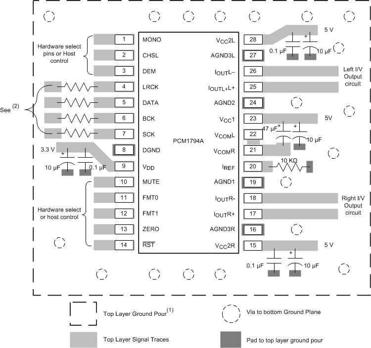
Place the decoupling capacitors as close to the Vcc1, VCC2L, VCC2R, VCOML, VCOMR, and VDD pins as possible. See Figure 34 for additional guidelines.

10.2 Layout Example
PCM1794A layout_sles117.gif
1. TI recommends to place a top layer ground pour for shielding around device and connect it to the lower main PCB ground plane with multiple vias.
2. These resistors help prevent overshoot and reduce coupling. Begin with a value of 10 Ω for the MCLK resistor and
27 Ω for the other resistors.
Figure 34. PCM1794A Layout Example