ZHCSK39C August 2019 – August 2020 OPA862
PRODUCTION DATA
- 1 特性
- 2 应用
- 3 说明
- 4 Revision History
- 5 Pin Configuration and Functions
-
6 Specifications
- 6.1 Absolute Maximum Ratings
- 6.2 ESD Ratings
- 6.3 Recommended Operating Conditions
- 6.4 Thermal Information
- 6.5 Electrical Characteristics: VS = ±2.5 V to ±5 V
- 6.6 Typical Characteristics: VS = ±5 V
- 6.7 Typical Characteristics: VS = ±2.5 V
- 6.8 Typical Characteristics: VS = 1.9 V, –1.4 V
- 6.9 Typical Characteristics: VS = 1.9 V, –1.4 V to ±5 V
- 7 Detailed Description
- 8 Application and Implementation
- 9 Power Supply Recommendations
- 10Layout
- 11Device and Documentation Support
- 12Mechanical, Packaging, and Orderable Information
7.3.2 Anti-Phase Reversal Protection
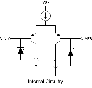
When the input common-mode voltage approaches or exceeds VS–, the base-collector junction of the input transistors forward biases. This condition creates an output path parallel to the normal gm path of the transistors that is opposite in phase to the gm path. When this parallel path starts to dominate, phase inversion occurs. To protect against phase inversion, the OPA862 features anti-phase reversal (APR) protection Schottky diodes on the input transistors. The Schottky diodes turn on at a voltage lower than the forward bias voltage of the base-collector junction, thus preventing the forward bias and the phase-inversion at the base-collector junction of the input transistors. Figure 7-2 shows a diagram of APR protection within the OPA862.
 Figure 7-2 Anti-Phase Reversal Protection