ZHCSFQ4 December 2016 OPA2836-Q1
PRODUCTION DATA.
- 1 特性
- 2 应用
- 3 说明
- 4 修订历史记录
- 5 OPA2836-Q1 Related Devices
- 6 Pin Configuration and Functions
- 7 Specifications
- 8 Detailed Description
-
9 Application and Implementation
- 9.1
Application Information
- 9.1.1 Noninverting Amplifier
- 9.1.2 Inverting Amplifier
- 9.1.3 Instrumentation Amplifier
- 9.1.4 Attenuators
- 9.1.5 Single-Ended-to-Differential Amplifier
- 9.1.6 Differential-to-Signal-Ended Amplifier
- 9.1.7 Differential-to-Differential Amplifier
- 9.1.8 Pulse Application With Single-Supply
- 9.1.9 ADC Driver Performance
- 9.2 Typical Applications
- 9.1
Application Information
- 10Power Supply Recommendations
- 11Layout
- 12器件和文档支持
- 13机械、封装和可订购信息
9 Application and Implementation
NOTE
Information in the following applications sections is not part of the TI component specification, and TI does not warrant its accuracy or completeness. TI’s customers are responsible for determining suitability of components for their purposes. Customers should validate and test their design implementation to confirm system functionality.
9.1 Application Information
9.1.1 Noninverting Amplifier
The OPA2836-Q1 can be used as a noninverting amplifier with a signal input to the noninverting input, VIN+ . A basic block diagram of the circuit is illustrated in Figure 51.
If VIN = VREF + VSIG, then the output of the amplifier can be calculated according to Equation 1.

The signal gain of the circuit is set by  , and VREF provides a reference around which the input and output signals swing. Output signals are in-phase with the input signals.
The OPA2836-Q1 is designed for the nominal value of RF to be 1 kΩ in gains other than +1. This value gives excellent distortion performance, maximum bandwidth, best flatness, and best pulse response. RF = 1 kΩ must be used as a default unless other design goals require changing to other values. All test circuits used to collect data for this document have RF = 1 kΩ for all gains other than +1. Gain of +1 is a special case where RF is shorted and RG is left open.
9.1.2 Inverting Amplifier
The OPA2836-Q1 can be used as an inverting amplifier with a signal input to the inverting input, VIN– , through the gain setting resistor RG. A basic block diagram of the circuit is illustrated in Figure 52.
If VIN = VREF + VSIG, then the output of the amplifier may be calculated according to Equation 2.

The signal gain of the circuit is set by:  , and VREF provides a reference point around which the input and output signals swing. Output signals are 180° out-of-phase with the input signals. The nominal value of RF must be 1 kΩ for inverting gains.
9.1.3 Instrumentation Amplifier
Figure 62 is an instrumentation amplifier that combines the high input impedance of the differential-to-differential amplifier circuit and the common-mode rejection of the differential-to-single-ended amplifier circuit. This circuit is often used in applications where high input impedance is required (such as taps from a differential line or in cases where the signal source has a high output impedance).
If VIN+ = VCM + VSIG+ and VIN– = VCM + VSIG– , then the output of the amplifier can be calculated according to Equation 3.

The signal gain of the circuit is set by  . VCM is rejected and VREF provides a level shift around which the output signal swings. The single-ended output signal is in-phase with the differential input signal.
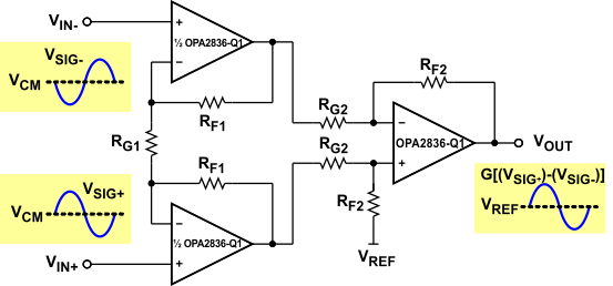 Figure 62. Instrumentation Amplifier
Integrated solutions are available, but the OPA2836-Q1 provides a much lower-power, high-frequency solution. For best CMRR performance, resistors must be matched. Given that CMRR ≈ the resistor tolerance, a 0.1% tolerance provides apprximately 60-dB CMRR.
9.1.4 Attenuators
The noninverting circuit of Figure 51 has a minimum gain of 1. To implement attenuation, a resistor divider can be placed in series with the positive input, and the amplifier can be set for a gain of 1 by shorting VOUT to VIN– and removing RG. Because the operational amplifier input has high input impedance, the attenuation is set by the resistor divider.
The inverting circuit of Figure 52 can be used as an attenuator by making RG larger than RF. The attenuation is simply the resistor ratio. For example, a 10:1 attenuator can be implemented with RF = 1 kΩ and RG = 10 kΩ.
9.1.5 Single-Ended-to-Differential Amplifier
Figure 63 illustrates an amplifier circuit that is used to convert single-ended signals to differential and that provides gain and level shifting. This circuit can be used for converting signals to differential in applications (such as line drivers for Cat5 cabling or for driving differential-input SAR and ΔΣ ADCs).
With VIN = VREF + VSIG , the output of the amplifier can be calculated according to Equation 4.

The differential-signal gain of the circuit is 2 × G, and VREF provides a reference around which the output signal swings. The differential output signal is in-phase with the single-ended input signal.
 Figure 63. Single-Ended-to-Differential Amplifier
Line termination on the output can be accomplished with resistors RO. The differential input impedance of the circuit is 2 × RO. For example, if a 100-Ω Cat5 cable is used with double termination, the amplifier is typically set for a differential gain of 2 V/V (6 dB) with RF = 0 Ω (short), RG = open, 2R = 1 kΩ, R1 = 0 Ω, R = 499 Ω to balance the input bias currents, and RO = 49.9 Ω for output line termination. This configuration is shown in Figure 64.
For driving a differential-input ADC, the situation is similar but the output resistors (RO) are typically chosen along with a capacitor across the ADC input for optimum filtering and settling-time performance.
 Figure 64. Cat5 Line Driver With Gain = 2 V/V (6 dB)
9.1.6 Differential-to-Signal-Ended Amplifier
Figure 65 illustrates a differential amplifier that converts differential signals to single-ended and provides gain (or attenuation) and level shifting. This circuit can be used in applications such as a line receiver for converting a differential signal from a Cat5 cable to single ended.
If VIN+ = VCM + VSIG+ and VIN– = VCM + VSIG–, then the output of the amplifier can be calculated according to Equation 5.

The signal gain of the circuit is set by  . VCM is rejected, and VREF provides a level shift around which the output signal swings. The single-ended output signal is in-phase with the differential input signal.
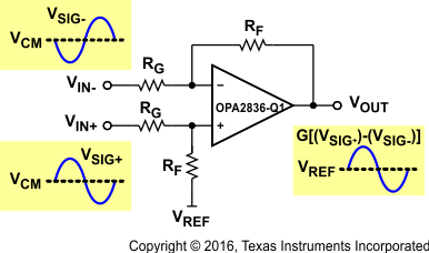 Figure 65. Differential to Single Ended Amplifier
Line termination can be accomplished with a resistor shunt across the input. The differential input impedance of the circuit is the resistor value in parallel with the amplifier circuit. For low-gain and low-line impedance, the resistor value to add is approximately the impedance of the line. For example, if a 100-Ω Cat5 cable is used with a gain of 1 amplifier and RF = RG = 1 kΩ, adding a 100-Ω shunt across the input gives a differential impedance of 98 Ω that is adequate for most applications.
For best CMRR performance, resistors must be matched. A rule of thumb is CMRR ≈ the resistor tolerance; so a 0.1% tolerance provides approximately 60-dB CMRR.
9.1.7 Differential-to-Differential Amplifier
Figure 66 shows a differential amplifier that is used to amplify differential signals. This circuit has high input impedance and is often used in differential line driver applications where the signal source is a high-impedance driver (for example, a differential DAC) that must drive a line.
If VIN± = VCM + VSIG± , then the output of the amplifier can be calculated according to Equation 6.

The signal gain of the circuit is set by  , and VCM passes with unity gain. The amplifier in essence combines two noninverting amplifiers into one differential amplifier with the RG resistor shared, which makes RG effectively half the value when calculating the gain. The output signals are in-phase with the input signals.
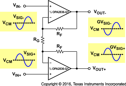 Figure 66. Differential to Differential Amplifier
9.1.8 Pulse Application With Single-Supply
For pulsed applications, where the signal is at ground and pulses to some positive or negative voltage, the circuit bias-voltage considerations are different than with a signal that swings symmetrical about a reference point. Figure 67 shows a pulsed situation where the signal is at ground (0 V) and pulses to a positive value.
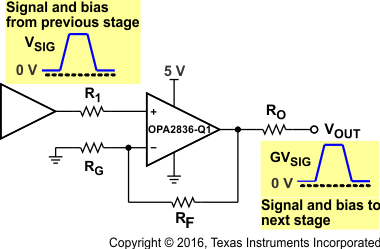 Figure 67. Noninverting Single Supply With Pulse
If the input signal pulses negatively from ground, an inverting amplifier is more appropriate, as shown in Figure 68. A key consideration in both noninverting and inverting cases is that the input and output voltages are kept within the limits of the amplifier; because the VICR of the OPA2836-Q1 includes the negative supply rail, the OPA2836-Q1 lends itself to this application.
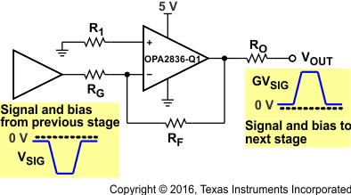 Figure 68. Inverting Single Supply With Pulse
9.1.9 ADC Driver Performance
The OPA2836-Q1 provides excellent performance when driving high-performance, delta-sigma (ΔΣ), and successive approximation register (SAR) ADCs in low-power audio and industrial applications.
To show achievable performance, the OPA2836-Q1 is tested as the drive amplifier for the ADS8326. The ADS8326 is a 16-bit, micro power, SAR ADC with pseudo-differential inputs and sample rates up to 250 kSPS. The ADS8326 offers excellent noise and distortion performance in a small 8-pin SOIC or VSSOP (MSOP) package. Low power and small size make the ADS8326 and OPA2836-Q1 devices an ideal solution for portable and battery-operated systems, for remote data-acquisition modules, simultaneous multichannel systems, and isolated data acquisition.
The circuit shown in Figure 69 is used to test the performance. Figure 70 is the FFT plot showing the spectral performance with a 10-kHz input frequency, and Table 3 shows the tabulated ac analysis results.
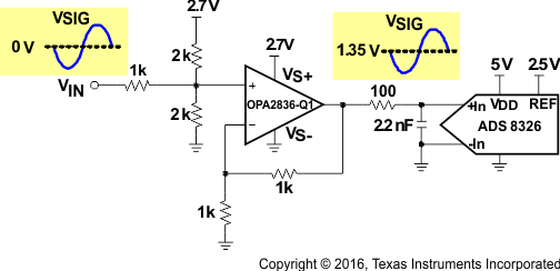 Figure 69. OPA2836-Q1 and ADS8326 Test Circuit
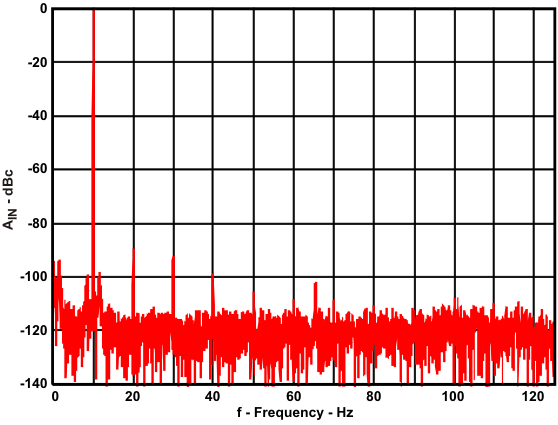 Figure 70. ADS8326 and OPA2836-Q1 10-kHz FFT
Table 3. AC Analysis
| TONE (kHz) | SIGNAL (dBFS) | SNR (dBc) | THD (dBc) | SINAD (dBc) | SFDR (dBc) |
|---|---|---|---|---|---|
| 10 | –0.85 | 83.3 | –86.6 | 81.65 | 88.9 |
9.2 Typical Applications
9.2.1 Audio-Frequency Performance
The OPA2836-Q1 provides excellent audio performance with very low quiescent power. To show performance in the audio band, a 2700 series audio analyzer from Audio Precision is used to test THD+N and FFT at 1-VRMS output voltage.
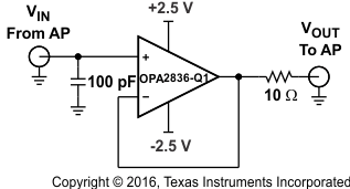
Figure 71 shows the test circuit used for the audio-frequency performance application.
9.2.1.1 Design Requirements
Design a low distortion, single-ended input to single-ended output audio amplifier using the OPA2836-Q1. The 2700 series audio analyzer from Audio Precision is used as the signal source and also as the measurement system.
Table 4. Design Requirements
| CONFIGURATION | INPUT EXCITATION |
PERFORMANCE TARGET |
RLoad |
|---|---|---|---|
| OPA2836-Q1 unity-gain configuration | 1-kHz tone frequency | > 110 dBc SFDR | 300 Ω and 100 kΩ |
9.2.1.2 Detailed Design Procedure
The OPA2836-Q1 is tested in this application in a unity-gain buffer configuration. A buffer configuration is chosen because this configuration maximizes the loop gain of the amplifier configuration. At higher closed-loop gains, the loop gain of the circuit reduces, resulting in degraded harmonic distortion. The relationship between distortion and closed-loop gain at a fixed input frequency is illustrated in Figure 35 in the Typical Characteristics section. The test was performed under varying output load conditions using a resistive load of 300 Ω and 100 kΩ. Figure 33 illustrates the distortion performance of the amplifier versus output resistive load. Output loading, output swing, and closed-loop gain play a key role in determining the distortion performance of the amplifier.
NOTE
The 100-pF capacitor to ground on the input helped to decouple noise pickup in the lab and improved noise performance.
The Audio Precision was configured as a single-ended output in this application circuit. In applications where a differential output is available, the OPA2836-Q1 device can be configured as a differential-to-single-ended amplifier; see Figure 65. Power-supply bypassing is critical in order to reject noise from the power supplies. A 2.2-μF power-supply decoupling capacitor must be placed within 2 inches of the device and can be shared with other operational amplifiers on the same board. A 0.1-μF power supply decoupling capacitor must be placed as close to the power supply pins as possible, preferably within 0.1 inch. For split supply, a capacitor is required for both supplies. A 0.1-µF capacitor placed directly between the supplies is also beneficial for improving system noise performance. If the output load is very heavy, in the order of 16 Ω to 32 Ω, performance of the amplifier can begin to degrade. In order to drive such heavy loads, both channels of the OPA2836-Q1 device can be paralleled with the outputs isolated with 1-Ω resistors to reduce the loading effects.
9.2.1.3 Application Curves
A 10-Ω series resistor can be inserted between the capacitor and the noninverting pin to isolate the capacitance.
Figure 72 shows the THD+N performance with 100-kΩ and 300-Ω loads, with A-weighting and with no weighting. Both loads show similar performance. With no weighting, the THD+N performance is dominated by the noise; whereas, A-weighting provides filtering that improves the noise.
Figure 73 and Figure 74 show FFT outputs with a 1-kHz tone and 100-kΩ and 300-Ω loads. To show relative performance of the device versus the test set, one channel has the OPA2836-Q1 in-line between generator output and analyzer input and the other channel is in Gen Mon loopback mode that internally connects the signal generator to the analyzer input. With a 100-kΩ load, Figure 73, the curves are basically indistinguishable from each other except for noise, meaning that the OPA2836-Q1 cannot be directly measured. With a 300-Ω load, Figure 74, the main difference between the curves is that the OPA2836-Q1 shows slightly higher even-order harmonics, but odd-order harmonics are masked by the test-set performance.
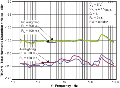 Figure 72. OPA2836-Q1 1 VRMS, 20-Hz to 80-kHz THD+N
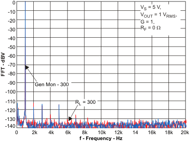 Figure 74. OPA2836-Q1 and AP Gen Mon 10-kHz FFT Plot;
 VOUT = 1 VRMS, RL = 300 Ω
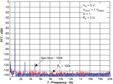 Figure 73. OPA2836-Q1 and AP Gen Mon 10-kHz FFT Plot; VOUT = 1 VRMS, RL = 100 kΩ
9.2.2 Active Filters
The OPA2836-Q1 can be used to design active filters. Figure 75 and Figure 76 show MFB and Sallen-Key circuits designed using the WEBENCH® filter designer to implement second-order low-pass Butterworth filter circuits. Figure 77 shows the frequency response.
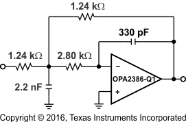 Figure 75. MFB 100-kHz Second Order Low-Pass Butterworth Filter Circuit
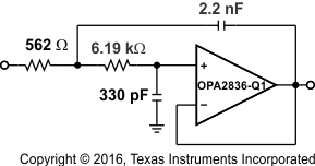 Figure 76. Sallen-Key 100-kHz Second Order Low-Pass Butterworth Filter Circuit
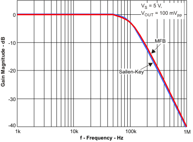 Figure 77. MFB and Sallen-Key Second Order Low-Pass Butterworth Filter Response
MFB and Sallen-Key filter circuits offer similar performance. The main difference is the MFB uses an inverting amplifier in the pass-band and the Sallen-Key uses an noninverting amplifier. The primary advantage for each is the Sallen-Key in unity gain has no resistor gain-error term, and thus no sensitivity to gain error, whereas the MFB has inherently better attenuation properties beyond the bandwidth of the operational amplifier.