ZHCSED2 November 2015 OPA2211-EP
PRODUCTION DATA.
7 Detailed Description
7.1 Overview
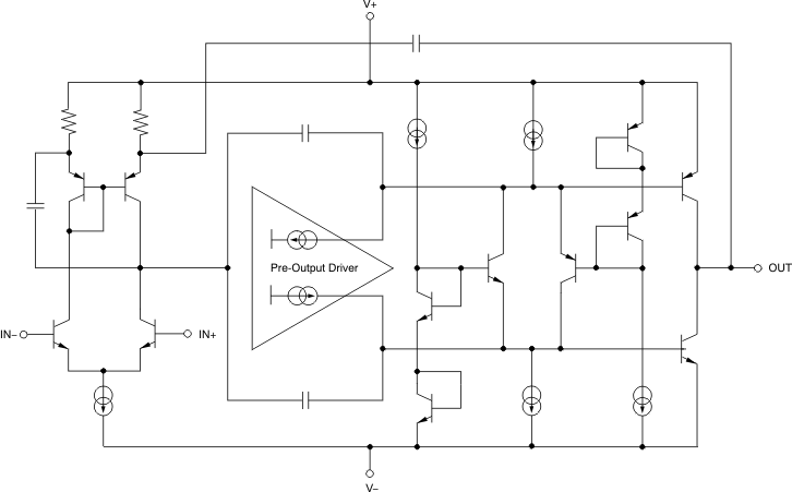
The OPA2211-EP is a unity-gain stable, precision operational amplifier with very low noise. Applications with noisy or high-impedance power supplies require decoupling capacitors close to the device pins. In most cases, 0.1-μF capacitors are adequate. Functional Block Diagram shows a simplified schematic of the OPA2211-EP. This die uses a SiGe bipolar process and contains 180 transistors.
7.2 Functional Block Diagram

7.3 Feature Description
7.3.1 Input Protection
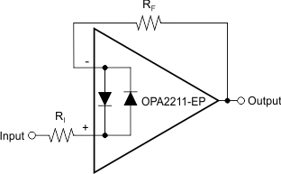
The input terminals of the OPA2211-EPFigure 38 are protected from excessive differential voltage with back-to-back diodes, as shown in . In most circuit applications, the input protection circuitry has no consequence. However, in low-gain or G = 1 circuits, fast ramping input signals can forward bias these diodes because the output of the amplifier cannot respond rapidly enough to the input ramp. This effect is illustrated in Figure 29 in the Typical Characteristics. If the input signal is fast enough to create this forward bias condition, the input signal current must be limited to 10 mA or less. If the input signal current is not inherently limited, an input series resistor can be used to limit the signal input current. This input series resistor degrades the low-noise performance of the OPA2211-EP, and is discussed in Noise Performance. Figure 38 shows an example implementing a current-limiting feedback resistor.
 Figure 38. Pulsed Operation
7.3.2 Noise Performance
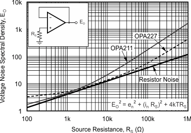
Figure 39 shows total circuit noise for varying source impedances with the operational amplifier in a unity-gain configuration (no feedback resistor network, and therefore no additional noise contributions). Two different operational amplifiers are shown with total circuit noise calculated. The OPA2211-EP has very low voltage noise, making it ideal for low source impedances (<2 kΩ). A similar precision operational amplifier, the OPA227, has somewhat higher voltage noise but lower current noise. It provides excellent noise performance at moderate source impedance (10 kΩ to 100 kΩ). Above 100 kΩ, a FET-input operational amplifier such as the OPA132 (very-low current noise) may provide improved performance. The equation in Figure 39 is shown for the calculation of the total circuit noise. Note that en = voltage noise, In = current noise, RS = source impedance, k = Boltzmann’s constant = 1.38 × 10⁻²³ J/K, and T is temperature in K.
 Figure 39. Noise Performance of the OPA2211-EP and OPA227 in Unity-Gain Buffer Configuration
7.3.3 Basic Noise Calculations
Design of low-noise operational amplifier circuits requires careful consideration of a variety of possible noise contributors: noise from the signal source, noise generated in the operational amplifier, and noise from the feedback network resistors. The total noise of the circuit is the root-sum-square combination of all noise components.
The resistive portion of the source impedance produces thermal noise proportional to the square root of the resistance. This function is plotted in Figure 39. The source impedance is usually fixed; consequently, select the operational amplifier and the feedback resistors to minimize the respective contributions to the total noise.
Figure 39 depicts total noise for varying source impedances with the operational amplifier in a unity-gain configuration (no feedback resistor network, and therefore no additional noise contributions). The operational amplifier itself contributes both a voltage noise component and a current noise component. The voltage noise is commonly modeled as a time-varying component of the offset voltage. The current noise is modeled as the time-varying component of the input bias current and reacts with the source resistance to create a voltage component of noise. Therefore, the lowest noise operational amplifier for a given application depends on the source impedance. For low source impedance, current noise is negligible and voltage noise generally dominates. For high source impedance, current noise may dominate.
Figure 41 shows both inverting and noninverting operational amplifier circuit configurations with gain. In circuit configurations with gain, the feedback network resistors also contribute noise. The current noise of the operational amplifier reacts with the feedback resistors to create additional noise components. The feedback resistor values can generally be chosen to make these noise sources negligible. The equations for total noise are shown for both configurations.
7.3.4 Total Harmonic Distortion Measurements
OPA2211-EP series operational amplifiers have excellent distortion characteristics. THD + Noise is below 0.0002% (G = +1, VOUT = 3 VRMS) throughout the audio frequency range, 20 Hz to 20 kHz, with a 600-Ω load.
The distortion produced by OPA2211-EP series operational amplifiers is below the measurement limit of many commercially available distortion analyzers. However, a special test circuit illustrated in Figure 42 can be used to extend the measurement capabilities.
Operational amplifier distortion can be considered an internal error source that can be referred to the input. Figure 42 shows a circuit that causes the operational amplifier distortion to be 101 times greater than that normally produced by the operational amplifier. The addition of R3 to the otherwise standard noninverting amplifier configuration alters the feedback factor or noise gain of the circuit. The closed-loop gain is unchanged, but the feedback available for error correction is reduced by a factor of 101, thus extending the resolution by 101. Note that the input signal and load applied to the operational amplifier are the same as with conventional feedback without R3. The value of R3 should be kept small to minimize its effect on the distortion measurements.
Validity of this technique can be verified by duplicating measurements at high gain and/or high frequency where the distortion is within the measurement capability of the test equipment. Measurements for this data sheet were made with an Audio Precision System Two distortion/noise analyzer, which greatly simplifies such repetitive measurements. The measurement technique can, however, be performed with manual distortion measurement instruments.
7.4 Device Functional Modes
The OPAx211 has a single functional mode and is operational when the power-supply voltage is greater than 4.5 V (±2.25 V). The maximum power supply voltage for the OPAx211 is 36 V (±18 V).