ZHCSPS9C june 2022 – july 2023 OPA186 , OPA2186 , OPA4186
PRODUCTION DATA
- 1
- 1 特性
- 2 应用
- 3 说明
- 4 Revision History
- 5 Pin Configuration and Functions
- 6 Specifications
- 7 Detailed Description
- 8 Application and Implementation
- 9 Device and Documentation Support
- 10Mechanical, Packaging, and Orderable Information
8.2.1.2 Detailed Design Procedure
Designing a high-side current monitor circuit is straightforward, provided that the amplifier electrical characteristics are carefully considered so that linear operation is maintained. Other additional characteristics, such as the input voltage range of the analog to digital converter (ADC) that follows the current monitor stage, must also be considered when configuring the system.
For example, consider the design of a OPAx186 high-side current monitor with an output voltage range set to be compatible with the input of an ADC with an input range of 3.3 V, such as one integrated in a microcontroller. The full-scale input range of this converter is 0 V to 3.3 V. Although the OPAx186 is specified as a rail-to-rail input/output (RRIO) amplifier, the linear output operating range (like all amplifiers) does not quite extend all the way to the supply rails. This linear operating range must be considered.
In this design example, the OPAx186 is powered by 24 V; therefore, the device is easily capable of providing the 3.3-V positive level; or even more, if the ADC has a wider input range. However, because the OPAx186 output does not swing completely to 0 V, the specified lower swing limit must be observed in the design.
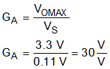
The best measure of an op-amp linear output voltage range comes from the open-loop voltage gain (AOL) specification listed in the Electrical Characteristics table. The AOL test conditions specify a linear swing range 300 mV from each supply rail (RL = 10 kΩ). Therefore, the linear swing limit on the low end (VoMIN) is 300 mV, and 3.3 V is the VoMAX limit, thus yielding an 11:1 VoMAX to VoMIN ratio. This ratio proves important in determining the difference amplifier operating parameters.
A nominal load current (IL) of 10 A is used in this example. In most applications, however, the ability to monitor current levels far less than 10 A is useful. This situation is where the 11:1 VoMAX to VoMIN ratio is crucial. If 11 A is set as the maximum current, this current must correspond to a 3.3-V output. Using the 11:1 ratio, the minimum current of 1 A corresponds to 300 mV.
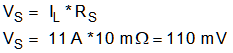
Selection of current sense resistor RS comes down to how much voltage drop can be tolerated at maximum current and the permissible power loss or dissipation. A good compromise for a 10-A sense application is an RS of 10 mΩ. That value results in a power dissipation of 1 W, and a 0.1-V drop at 10 A.
Next, determine the gain of the OPAx186 difference amplifier circuit. The maximum current of 11 A flowing through a 10-mΩ sense resistor results in 110 mV across the resistor. That voltage appears as a differential voltage, VR, that is applied across the OPAx186 difference amplifier circuit inputs:
The OPAx186 required voltage gain is determined from:
Now, checking the VoMIN using IL = 1 A:
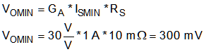
Figure 8-3 shows the complete OPAx186 high-side current monitor. The circuit is capable of monitoring a current range of < 1 A to 11 A, with a VCM very close to the 24-V supply voltage.
 Figure 8-3 OPAx186 Configured as a High-Side Current Monitor
In this example, the OPAx186 output voltage is intentionally limited to 3.3 V. However, because of the 24-V supply, the output voltage can be much higher to allow for a higher-voltage data converter with a higher dynamic range.
The circuit in Figure 8-3 was checked using the TINA Spice circuit simulation tool to verify the correct operation of the OPAx186 high-side current monitor. The simulation results are seen in Figure 8-4. The performance is exactly as expected. Upon careful inspection of the plots, one possible surprise is that VO continues towards zero as the sense current drops below 1 A, where VO is 300 mV and less.
Figure 8-4 OPAx186 High-Side Current-Monitor Simulation SchematicThe OPAx186 output, as well as other CMOS output amplifiers, often swing closer to 0 V than the linear output parameters suggest. The voltage output swing, VO (see the Electrical Characteristics table), is not an indication of the linear output range, but rather how close the output can move towards the supply rail. In that region, the amplifier output approaches saturation, and the amplifier ceases to operate linearly. Thus, in the current-monitor application, the current-measurement capability can continue to much less than the 300-mV output level. However, keep in mind that the linearity errors are becoming large.
Lastly, some notes about maximizing the high-side current monitor performance:
- All resistor values are critical for accurate gain results. Match resistor pairs of [R1 and R3] and [R2 and R4] as closely as possible to minimize common-mode mismatch error. Use a 0.1% tolerance, or better. Often, selecting two adjacent resistors on a reel provides close matching compared to random selection.
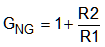
- Keep the closed-loop gain, GA, of the OPAx186 difference amplifier set to a reasonable value to reduce gain error and maximize bandwidth. A GA of 30 V/V is used in the example.
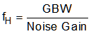
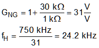
- Although current monitoring is often used for monitoring dc supply currents, ac current can also be monitored. The –3-dB bandwidth, or upper cutoff frequency, of the circuit is:
where
- GBW = the amplifier unity gain bandwidth; 750 kHz for the OPAx186.
- Noise Gain = the gain as seen going into the op-amp noninverting input, and is defined by:
For the OPAx186 circuit in Figure 8-3, the results are:
Make sure that the amplifier slew rate is sufficient to support the expected output voltage swing range and waveform. Also, if a single power supply (such as 24 V) is used, the ac power source applied to the sense input must have a positive dc component to keep the VCM greater than 0 V. To maintain normal operation, the input voltage cannot drop to less than 0 V.
The OPAx186 output can attain a 0‑V output level if a small negative voltage is used to power the V– pin instead of ground. The LM7705 is a switched capacitor voltage inverter with a regulated, low-noise, –0.23-V fixed voltage output. Powering the OPAx186 V– pin at this level approximately matches the 300‑mV linear output voltage swing lower limit, thus extending the output swing to 0 V, or very near 0 V. This configuration greatly improves the resolution at low sense current levels.
The LM7705 requires only about 78 μA of quiescent current, but be aware that the specified supply range is 3 V to 5.25 V. The 3.3-V or 5-V supply used by the ADC can be used as a power source.
For more information about amplifier-based, high-side current monitors, see the TI Analog Engineer’s Circuit Cookbook: Amplifiers.