ZHCSE47A September   2015  – June 2022 OPA1688

PRODUCTION DATA  

  1. 特性
  2. 应用
  3. 说明
  4. Revision History
  5. Device Comparison Table
  6. Pin Configuration and Functions
  7. Specifications
    1. 7.1 Absolute Maximum Ratings
    2. 7.2 ESD Ratings
    3. 7.3 Recommended Operating Conditions
    4. 7.4 Thermal Information
    5. 7.5 Electrical Characteristics
    6. 7.6 Typical Characteristics
  8. Detailed Description
    1. 8.1 Overview
    2. 8.2 Functional Block Diagram
    3. 8.3 Feature Description
      1. 8.3.1 EMI Rejection
      2. 8.3.2 Phase-Reversal Protection
      3. 8.3.3 Capacitive Load and Stability
    4. 8.4 Device Functional Modes
      1. 8.4.1 Common-Mode Voltage Range
      2. 8.4.2 Electrical Overstress
      3. 8.4.3 Overload Recovery
  9. Applications and Implementation
    1. 9.1 Application Information
    2. 9.2 Typical Application
      1. 9.2.1 Headphone Amplifier Circuit Configuration
        1. 9.2.1.1 Design Requirements
        2. 9.2.1.2 Detailed Design Procedure
        3. 9.2.1.3 Application Curves
  10. 10Power Supply Recommendations
  11. 11Layout
    1. 11.1 Layout Guidelines
    2. 11.2 Layout Example
  12. 12Device and Documentation Support
    1. 12.1 Device Support
      1. 12.1.1 Development Support
        1. 12.1.1.1 PSpice® for TI
        2. 12.1.1.2 TINA-TI™ Simulation Software (Free Download)
    2. 12.2 Documentation Support
      1. 12.2.1 Related Documentation
    3. 12.3 接收文档更新通知
    4. 12.4 支持资源
    5. 12.5 Trademarks
    6. 12.6 Electrostatic Discharge Caution
    7. 12.7 术语表
  13. 13Mechanical, Packaging, and Orderable Information

封装选项

机械数据 (封装 | 引脚)
散热焊盘机械数据 (封装 | 引脚)
订购信息

Capacitive Load and Stability

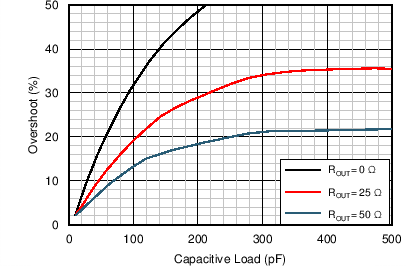
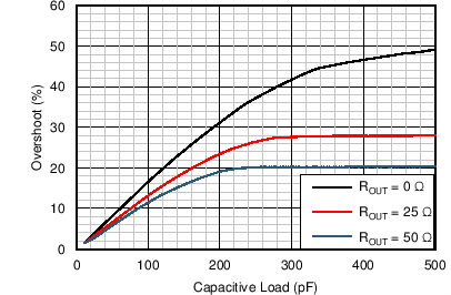
The dynamic characteristics of the OPA1688 are optimized for commonly-used operating conditions. The combination of low closed-loop gain and high capacitive loads decreases the phase margin of the amplifier and may lead to gain peaking or oscillations. As a result, heavier capacitive loads must be isolated from the output. The simplest way to achieve this isolation is to add a small resistor (for example, ROUT = 50 Ω) in series with the output. Figure 8-3 and Figure 8-4 show graphs of small-signal overshoot versus capacitive load for several values of ROUT; see the Feedback Plots Define Op Amp AC Performance application bulletin, available for download from www.ti.com, for details of analysis techniques and application circuits.
GUID-9F91D838-2392-498A-8355-69E58F6D91CF-low.png
G = –1
Figure 8-3 Small-Signal Overshoot vs Capacitive Load (100-mV Output Step)
GUID-A80CC8C6-78DA-4BED-A15A-9654C37C0851-low.png
G = 1
Figure 8-4 Small-Signal Overshoot vs Capacitive Load (100-mV Output Step)