ZHCSMS9J September 1973 – February 2025 NA555 , NE555 , SA555 , SE555
PRODUCTION DATA
- 1
- 1 特性
- 2 应用
- 3 说明
- 4 Pin Configuration and Functions
- 5 Specifications
- 6 Detailed Description
- 7 Applications and Implementation
- 8 Device and Documentation Support
- 9 Revision History
- 10Mechanical, Packaging, and Orderable Information
封装选项
请参考 PDF 数据表获取器件具体的封装图。
机械数据 (封装 | 引脚)
- D|8
- P|8
- PS|8
- PW|8
散热焊盘机械数据 (封装 | 引脚)
- PS|8
订购信息
6.3.1 Monostable Operation
For monostable operation, Figure 6-2 shows how to connect any of these timers. If the output is low, application of a negative-going pulse to the trigger (TRIG) sets the flip-flop ( Q goes low), drives the output high, and turns off Q1. Capacitor C is then charged through RA until the voltage across the capacitor reaches the threshold voltage of the threshold (THRES) input. If TRIG has returned to a high level, the output of the threshold comparator resets the flip-flop ( Q goes high), drives the output low, and discharges C through Q1.
 Figure 6-2 Circuit
for Monostable Operation
Figure 6-2 Circuit
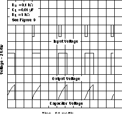
for Monostable OperationMonostable operation is initiated when the TRIG voltage is less than the trigger threshold. After being initiated, the sequence ends only if TRIG is high for at least 10µs before the end of the timing interval. When the trigger is grounded, the comparator storage time can be as long as 10µs, which limits the minimum monostable pulse width to 10µs. As a result of the threshold level and saturation voltage of Q1, the output pulse duration is approximately tw = 1.1 × RAC. Figure 6-4 is a plot of the time constant for various values of RA and C. The threshold levels and charge rates both are directly proportional to the supply voltage, VCC. The timing interval is, therefore, independent of the supply voltage, as long as the supply voltage is constant during the time interval.
 Figure 6-3 Typical Monostable Waveforms
 Figure 6-4 Output Pulse Duration vs Capacitance
Applying a negative-going trigger pulse simultaneously to RESET and TRIG during the timing interval discharges C and reinitiates the cycle, commencing on the positive edge of the reset pulse. The output is held low for as long as the reset pulse is low. To prevent false triggering, when RESET is not used, connect RESET to VCC.