ZHCSH48 April 2017 MSP430FR5989-EP
PRODUCTION DATA.
- 1器件概述
- 2修订历史记录
- 3Terminal Configuration and Functions
-
4 Specifications
- 4.1 Absolute Maximum Ratings
- 4.2 ESD Ratings
- 4.3 Recommended Operating Conditions
- 4.4 Active Mode Supply Current Into VCC Excluding External Current
- 4.5 Typical Characteristics, Active Mode Supply Currents
- 4.6 Low-Power Mode (LPM0, LPM1) Supply Currents Into VCC Excluding External Current
- 4.7 Low-Power Mode (LPM2, LPM3, LPM4) Supply Currents (Into VCC) Excluding External Current
- 4.8 Low-Power Mode With LCD Supply Currents (Into VCC) Excluding External Current
- 4.9 Low-Power Mode LPMx.5 Supply Currents (Into VCC) Excluding External Current
- 4.10 Typical Characteristics, Low-Power Mode Supply Currents
- 4.11 Typical Characteristics, Current Consumption per Module
- 4.12 Thermal Resistance Characteristics
- 4.13
Timing and Switching Characteristics
- 4.13.1 Power Supply Sequencing
- 4.13.2 Reset Timing
- 4.13.3 Clock Specifications
- 4.13.4 Wake-up Characteristics
- 4.13.5 Peripherals
- 4.13.6 Emulation and Debug
-
5Detailed Description
- 5.1 Overview
- 5.2 CPU
- 5.3 Operating Modes
- 5.4 Interrupt Vector Table and Signatures
- 5.5 Bootloader (BSL)
- 5.6 JTAG Operation
- 5.7 FRAM
- 5.8 RAM
- 5.9 Tiny RAM
- 5.10 Memory Protection Unit Including IP Encapsulation
- 5.11
Peripherals
- 5.11.1 Digital I/O
- 5.11.2 Oscillator and Clock System (CS)
- 5.11.3 Power-Management Module (PMM)
- 5.11.4 Hardware Multiplier (MPY)
- 5.11.5 Real-Time Clock (RTC_C)
- 5.11.6 Watchdog Timer (WDT_A)
- 5.11.7 System Module (SYS)
- 5.11.8 DMA Controller
- 5.11.9 Enhanced Universal Serial Communication Interface (eUSCI)
- 5.11.10 Extended Scan Interface (ESI)
- 5.11.11 Timer_A TA0, Timer_A TA1
- 5.11.12 Timer_A TA2
- 5.11.13 Timer_A TA3
- 5.11.14 Timer_B TB0
- 5.11.15 ADC12_B
- 5.11.16 Comparator_E
- 5.11.17 CRC16
- 5.11.18 CRC32
- 5.11.19 AES256 Accelerator
- 5.11.20 True Random Seed
- 5.11.21 Shared Reference (REF_A)
- 5.11.22 LCD_C
- 5.11.23 Embedded Emulation
- 5.11.24
Input/Output Diagrams
- 5.11.24.1 Digital I/O Functionality - Ports P1 to P10
- 5.11.24.2 Capacitive Touch Functionality Ports P1 to P10 and PJ
- 5.11.24.3 Port P1 (P1.0 to P1.3) Input/Output With Schmitt Trigger
- 5.11.24.4 Port P1 (P1.4 to P1.7) Input/Output With Schmitt Trigger
- 5.11.24.5 Port P2 (P2.0 to P2.3) Input/Output With Schmitt Trigger
- 5.11.24.6 Port P2 (P2.4 to P2.7) Input/Output With Schmitt Trigger
- 5.11.24.7 Port P3 (P3.0 to P3.7) Input/Output With Schmitt Trigger
- 5.11.24.8 Port P4 (P4.0 to P4.7) Input/Output With Schmitt Trigger
- 5.11.24.9 Port P5 (P5.0 to P5.7) Input/Output With Schmitt Trigger
- 5.11.24.10 Port P6 (P6.0 to P6.6) Input/Output With Schmitt Trigger
- 5.11.24.11 Port P6 (P6.7) Input/Output With Schmitt Trigger
- 5.11.24.12 Port P7 (P7.0 to P7.7) Input/Output With Schmitt Trigger
- 5.11.24.13 Port P8 (P8.0 to P8.3) Input/Output With Schmitt Trigger
- 5.11.24.14 Port P8 (P8.4 to P8.7) Input/Output With Schmitt Trigger
- 5.11.24.15 Port P9 (P9.0 to P9.3) Input/Output With Schmitt Trigger
- 5.11.24.16 Port P9 (P9.4 to P9.7) Input/Output With Schmitt Trigger
- 5.11.24.17 Port P10 (P10.0 to P10.2) Input/Output With Schmitt Trigger
- 5.11.24.18 Port PJ (PJ.4 and PJ.5) Input/Output With Schmitt Trigger
- 5.11.24.19 Port PJ (PJ.6 and PJ.7) Input/Output With Schmitt Trigger
- 5.11.24.20 Port PJ (PJ.0 to PJ.3) JTAG Pins TDO, TMS, TCK, TDI/TCLK, Input/Output With Schmitt Trigger
- 5.12 Device Descriptors (TLV)
- 5.13 Memory
- 5.14 Identification
- 6Applications, Implementation, and Layout
- 7器件和文档支持
- 8机械、封装和可订购信息
6 Applications, Implementation, and Layout
NOTE
Information in the following applications sections is not part of the TI component specification, and TI does not warrant its accuracy or completeness. TI’s customers are responsible for determining suitability of components for their purposes. Customers should validate and test their design implementation to confirm system functionality.
6.1 Device Connection and Layout Fundamentals
This section discusses the recommended guidelines when designing with the MSP430. These guidelines are to make sure that the device has proper connections for powering, programming, debugging, and optimum analog performance.
6.1.1 Power Supply Decoupling and Bulk Capacitors
TI recommends connecting a combination of a 1-µF plus a 100-nF low-ESR ceramic decoupling capacitor to each AVCC, DVCC, and ESIDVCC pin. Higher-value capacitors may be used but can impact supply rail ramp-up time. Decoupling capacitors must be placed as close as possible to the pins that they decouple (within a few millimeters). Additionally, TI recommends separated grounds with a single-point connection for better noise isolation from digital to analog circuits on the board and to achieve high analog accuracy.
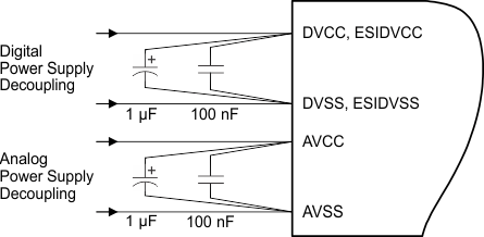 Figure 6-1 Power Supply Decoupling
6.1.2 External Oscillator
Depending on the device variant, the device can support a low-frequency crystal (32 kHz) on the LFXT pins, a high-frequency crystal on the HFXT pins, or both. External bypass capacitors for the crystal oscillator pins are required.
It is also possible to apply digital clock signals to the LFXIN and HFXIN input pins that meet the specifications of the respective oscillator if the appropriate LFXTBYPASS or HFXTBYPASS mode is selected. In this case, the associated LFXOUT and HFXOUT pins can be used for other purposes. If they are left unused, terminate them according to Section 3.4.
Figure 6-2 shows a typical connection diagram.
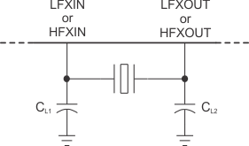 Figure 6-2 Typical Crystal Connection
See MSP430 32-kHz Crystal Oscillators for more information on selecting, testing, and designing a crystal oscillator with the MSP430 devices.
6.1.3 JTAG
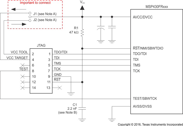
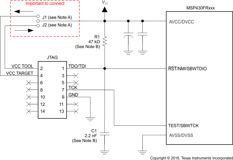
With the proper connections, the debugger and a hardware JTAG interface (such as the MSP-FET or MSP-FET430UIF) can be used to program and debug code on the target board. In addition, the connections also support the MSP-GANG production programmers, thus providing an easy way to program prototype boards, if desired. Figure 6-3 shows the connections between the 14-pin JTAG connector and the target device required to support in-system programming and debugging for 4-wire JTAG communication. Figure 6-4 shows the connections for 2-wire JTAG mode (Spy-Bi-Wire).
The connections for the MSP-FET and MSP-FET430UIF interface modules and the MSP-GANG are identical. Both can supply VCC to the target board (through pin 2). In addition, the MSP-FET and MSP-FET430UIF interface modules and MSP-GANG have a VCC sense feature that, if used, requires an alternate connection (pin 4 instead of pin 2). The VCC-sense feature senses the local VCC present on the target board (that is, a battery or other local power supply) and adjusts the output signals accordingly. Figure 6-3 and Figure 6-4 show a jumper block that supports both scenarios of supplying VCC to the target board. If this flexibility is not required, the desired VCC connections may be hard-wired to eliminate the jumper block. Pins 2 and 4 must not be connected at the same time.
For additional design information regarding the JTAG interface, see the MSP430 Hardware Tools User's Guide.
6.1.4 Reset
The reset pin can be configured as a reset function (default) or as an NMI function in the Special Function Register (SFR), SFRRPCR.
In reset mode, the RST/NMI pin is active low, and a pulse applied to this pin that meets the reset timing specifications generates a BOR-type device reset.
Setting SYSNMI causes the RST/NMI pin to be configured as an external NMI source. The external NMI is edge sensitive, and its edge is selectable by SYSNMIIES. Setting the NMIIE enables the interrupt of the external NMI. When an external NMI event occurs, the NMIIFG is set.
The RST/NMI pin can have either a pullup or pulldown that is enabled or not. SYSRSTUP selects either pullup or pulldown, and SYSRSTRE causes the pullup (default) or pulldown to be enabled (default) or not. If the RST/NMI pin is unused, it is required either to select and enable the internal pullup or to connect an external 47-kΩ pullup resistor to the RST/NMI pin with a 2.2-nF pulldown capacitor.
The pulldown capacitor should not exceed 2.2 nF when using devices with Spy-Bi-Wire mode or in 4-wire JTAG mode with TI tools like FET interfaces or GANG programmers. If JTAG or Spy-Bi-Wire access is not needed, up to a 10-nF pulldown capacitor may be used.
See the MSP430FR58xx, MSP430FR59xx, MSP430FR68xx, and MSP430FR69xx Family User's Guide for more information on the referenced control registers and bits.
6.1.5 Unused Pins
For details on the connection of unused pins, see Section 3.4.
6.1.6 General Layout Recommendations
- Proper grounding and short traces for external crystal to reduce parasitic capacitance. See MSP430 32-kHz Crystal Oscillators for recommended layout guidelines.
- Proper bypass capacitors on DVCC, AVCC, and reference pins if used.
- Avoid routing any high-frequency signal close to an analog signal line. For example, keep digital switching signals such as PWM or JTAG signals away from the oscillator circuit.
- See Circuit Board Layout Techniques for a detailed discussion of PCB layout considerations. This document is written primarily about op amps, but the guidelines are generally applicable for all mixed-signal applications.
- Proper ESD level protection should be considered to protect the device from unintended high-voltage electrostatic discharge. See MSP430 System-Level ESD Considerations for guidelines.
6.1.7 Do's and Don'ts
TI recommends powering the AVCC, DVCC, and ESIDVCC pins from the same source. At a minimum, during power up, power down, and device operation, the voltage difference between AVCC and DVCC must not exceed the limits specified in the Absolute Maximum Ratings section. Exceeding the specified limits may cause malfunction of the device including erroneous writes to RAM and FRAM.
6.2 Peripheral- and Interface-Specific Design Information
6.2.1 ADC12_B Peripheral
6.2.1.1 Partial Schematic
Figure 6-5 shows the recommended decoupling circuit when an external voltage reference is used.
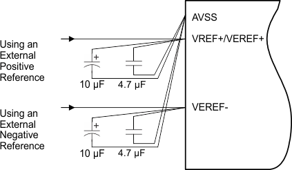 Figure 6-5 ADC12_B Grounding and Noise Considerations
6.2.1.2 Design Requirements
As with any high-resolution ADC, appropriate printed-circuit-board layout and grounding techniques should be followed to eliminate ground loops, unwanted parasitic effects, and noise.
Ground loops are formed when return current from the ADC flows through paths that are common with other analog or digital circuitry. If care is not taken, this current can generate small unwanted offset voltages that can add to or subtract from the reference or input voltages of the ADC. The general guidelines in Section 6.1.1 combined with the connections shown in Section 6.2.1.1 prevent this.
In addition to grounding, ripple and noise spikes on the power-supply lines that are caused by digital switching or switching power supplies can corrupt the conversion result. A noise-free design using separate analog and digital ground planes with a single-point connection is recommend to achieve high accuracy.
Figure 6-5 shows the recommended decoupling circuit when an external voltage reference is used. The internal reference module has a maximum drive current as specified in the Reference module's IO(VREF+) specification.
The reference voltage must be a stable voltage for accurate measurements. The capacitor values that are selected in the general guidelines filter out the high- and low-frequency ripple before the reference voltage enters the device. In this case, the 10-µF capacitor is used to buffer the reference pin and filter any low-frequency ripple. A bypass capacitor of 4.7 µF is used to filter out any high-frequency noise.
6.2.1.3 Detailed Design Procedure
For additional design information, see Designing With the MSP430FR58xx, FR59xx, FR68xx, and FR69xx ADC.
6.2.1.4 Layout Guidelines
Component that are shown in the partial schematic (see Figure 6-5) should be placed as close as possible to the respective device pins. Avoid long traces, because they add additional parasitic capacitance, inductance, and resistance on the signal.
Avoid routing analog input signals close to a high-frequency pin (for example, a high-frequency PWM), because the high-frequency switching can be coupled into the analog signal.
If differential mode is used for the ADC12_B, the analog differential input signals must be routed closely together to minimize the effect of noise on the resulting signal.
6.2.2 LCD_C Peripheral
6.2.2.1 Partial Schematic
Required LCD connections greatly vary by the type of display that is used (static or multiplexed), whether external or internal biasing is used, and also whether the on-chip charge pump is employed. For any display used, there is flexibility as to how the segment (Sx) and common (COMx) signals are connected to the MCU, which (assuming that the correct choices are made) can be advantageous for the PCB layout and for the design of the application software.
Because LCD connections are application specific, it is difficult to provide a single one-fits-all schematic. However, for an example of connecting a 4-mux LCD with 40 segment lines that has a total of 4 × 40 = 160 individually addressable LCD segments to an MSP430FR6989, see the Water Meter Reference Design for Two LC Sensors, Using Extended Scan Interface (ESI).
6.2.2.2 Design Requirements
Due to the flexibility of the LCD_C peripheral module to accommodate various segment-based LCDs, selecting the correct display for the application in combination with determining specific design requirements is often an iterative process. There can be well defined requirements in terms of how many individually addressable LCD segments need to be controlled, what the requirements for LCD contrast are, which device pins are available for LCD use, and which are required by other application functions, and what the power budget is, to name just a few. TI recommends reviewing the LCD_C peripheral module chapter in the MSP430FR58xx, MSP430FR59xx, MSP430FR68xx, and MSP430FR69xx Family User's Guide during the initial design requirements and decision process. Table 6-1 is a brief overview over different choices that can be made and their effects.
Table 6-1 LCD Features and Use Cases
| OPTION OR FEATURE | IMPACT OR USE CASE |
|---|---|
| Multiplexed LCD |
|
| Static LCD |
|
| Internal bias generation |
|
| External bias generation |
|
| Internal charge pump |
|
6.2.2.3 Detailed Design Procedure
A major component in designing the LCD solution is determining the exact connections between the LCD_C peripheral module and the display itself. Two basic design processes can be employed for this step, although in reality often a balanced co-design approach is recommended:
- PCB layout-driven design
- Software-driven design
In the PCB layout-driven design process, the segment Sx and common COMx signals are connected to respective MSP430 device pins so that the routing of the PCB can be optimized to minimize signal crossings and to keep signals on one side of the PCB only, typically the top layer. For example, using a multiplexed LCD, it is possible to arbitrarily connect the Sx and COMx signals between the LCD and the MSP430 device as long as segment lines are swapped with segment lines and common lines are swapped with common lines. It is also possible to not contiguously connect all segment lines but rather skip LCD_C module segment connections to optimize layout or to allow access to other functions that may be multiplexed on a particular device port pin. Employing a purely layout-driven design approach, however, can result in the LCD_C module control bits that are responsible for turning on and off segments to appear scattered throughout the memory map of the LCD controller (LCDMx registers). This approach potentially places a rather large burden on the software design that may also result in increased energy consumption due to the computational overhead required to work with the LCD.
The other extreme is a purely software-driven approach that starts with the idea that control bits for LCD segments that are frequently turned on and off together should be co-located in memory in the same LCDMx register or in adjacent registers. For example, in case of a 4-mux display that contains several 7-segment digits, from a software perspective it can be very desirable to control all 7 segments of each digit though a single byte-wide access to an LCDMx register. And consecutive segments are mapped to consecutive LCDMx registers. This allows use of simple look-up tables or software loops to output numbers on an LCD, reducing computational overhead and optimizing the energy consumption of an application. Establishing of the most convenient memory layout needs to be performed in conjunction with the specific LCD that is being used to understand its design constraints in terms of which segment and which common signals are connected to, for example, a digit.
For design information regarding the LCD controller input voltage selection including internal and external options, contrast control, and bias generation, see the LCD_C Controller chapter in the MSP430FR58xx, MSP430FR59xx, MSP430FR68xx, and MSP430FR69xx Family User's Guide.
For additional design information, see Designing With MSP430 and Segment LCDs.
6.2.2.4 Layout Guidelines
LCD segment (Sx) and common (COMx) signal traces are continuously switching while the LCD is enabled and should, therefore, be kept away from sensitive analog signals such as ADC inputs to prevent any noise coupling. TI recommends keeping the LCD signal traces on one side of the PCB grouped together in a bus-like fashion. A ground plane underneath the LCD traces and guard traces employed alongside the LCD traces can provide shielding.
If the internal charge pump of the LCD module is used, the externally provided capacitor on the LCDCAP pin should be located as close as possible to the MCU. The capacitor should be connected to the device using a short and direct trace and also have a solid connection to the ground plane that is supplying the VSS pins of the MCU.
For an example layout of connecting a 4-mux LCD with 40 segments to an MSP430FR6989 and using the charge pump feature, see Water Meter Reference Design for Two LC Sensors, Using Extended Scan Interface (ESI).