SNVSB23 March 2018 LP87521-Q1 , LP87522-Q1 , LP87523-Q1 , LP87524-Q1 , LP87525-Q1
PRODUCTION DATA.
- 1 Features
- 2 Applications
- 3 Description
- 4 Revision History
- 5 Device Comparison Table
- 6 Pin Configuration and Functions
- 7 Specifications
-
8 Detailed Description
- 8.1 Overview
- 8.2 Functional Block Diagram
- 8.3
Feature Descriptions
- 8.3.1 Multi-Phase DC/DC Converters
- 8.3.2 Sync Clock Functionality
- 8.3.3 Power-Up
- 8.3.4 Regulator Control
- 8.3.5 Enable and Disable Sequences
- 8.3.6 Device Reset Scenarios
- 8.3.7 Diagnosis and Protection Features
- 8.3.8 GPIO Signal Operation
- 8.3.9 Digital Signal Filtering
- 8.4 Device Functional Modes
- 8.5 Programming
- 8.6
Register Maps
- 8.6.1
Register Descriptions
- 8.6.1.1 OTP_REV
- 8.6.1.2 BUCK0_CTRL1
- 8.6.1.3 BUCK1_CTRL1
- 8.6.1.4 BUCK2_CTRL1
- 8.6.1.5 BUCK3_CTRL1
- 8.6.1.6 BUCK0_VOUT
- 8.6.1.7 BUCK0_FLOOR_VOUT
- 8.6.1.8 BUCK1_VOUT
- 8.6.1.9 BUCK1_FLOOR_VOUT
- 8.6.1.10 BUCK2_VOUT
- 8.6.1.11 BUCK2_FLOOR_VOUT
- 8.6.1.12 BUCK3_VOUT
- 8.6.1.13 BUCK3_FLOOR_VOUT
- 8.6.1.14 BUCK0_DELAY
- 8.6.1.15 BUCK1_DELAY
- 8.6.1.16 BUCK2_DELAY
- 8.6.1.17 BUCK3_DELAY
- 8.6.1.18 GPIO2_DELAY
- 8.6.1.19 GPIO3_DELAY
- 8.6.1.20 RESET
- 8.6.1.21 CONFIG
- 8.6.1.22 INT_TOP1
- 8.6.1.23 INT_TOP2
- 8.6.1.24 INT_BUCK_0_1
- 8.6.1.25 INT_BUCK_2_3
- 8.6.1.26 TOP_STAT
- 8.6.1.27 BUCK_0_1_STAT
- 8.6.1.28 BUCK_2_3_STAT
- 8.6.1.29 TOP_MASK1
- 8.6.1.30 TOP_MASK2
- 8.6.1.31 BUCK_0_1_MASK
- 8.6.1.32 BUCK_2_3_MASK
- 8.6.1.33 SEL_I_LOAD
- 8.6.1.34 I_LOAD_2
- 8.6.1.35 I_LOAD_1
- 8.6.1.36 PGOOD_CTRL1
- 8.6.1.37 PGOOD_CTRL2
- 8.6.1.38 PGOOD_FLT
- 8.6.1.39 PLL_CTRL
- 8.6.1.40 PIN_FUNCTION
- 8.6.1.41 GPIO_CONFIG
- 8.6.1.42 GPIO_IN
- 8.6.1.43 GPIO_OUT
- 8.6.1
Register Descriptions
- 9 Application and Implementation
- 10Power Supply Recommendations
- 11Layout
- 12Device and Documentation Support
- 13Mechanical, Packaging, and Orderable Information
8.3.5 Enable and Disable Sequences
The LP8752x-Q1 device supports start-up and shutdown sequencing with programmable delays for different regulator outputs using one EN1, EN2, EN3 control signal. The regulator is selected for delayed control with:
- EN_BUCKx = 1 (in BUCKx_CTRL1 register)
- EN_PIN_CTRLx = 1 (in BUCKx_CTRL1 register)
- EN_ROOF_FLOORx = 0 (in BUCKx_CTRL1 register)
- BUCKx_VSET[7:0] = Required voltage when ENx is high (in BUCKx_VOUT register)
- The ENABLE pin for control is selected with BUCKx_EN_PIN_SELECT[1:0] (in BUCKx_CTRL1 register)
- The delay from rising edge of ENx signal to the regulator enable is set by BUCKx_STARTUP_DELAY[3:0] bits (in BUCKx_DELAY register) and
- The delay from falling edge of ENx signal to the regulator disable is set by BUCKx_SHUTDOWN_DELAY[3:0] bits (in BUCKx_DELAY register)
There are four time steps available for start-up and shutdown sequences. The delay times are selected with DOUBLE_DELAY bit in CONFIG register and HALF_DELAY bit in PGOOD_CTRL2 register as shown in Table 4.
Table 4. Start-up and Shutdown Delays
| X_STARTUP_DELAY or
X_SHUTDOWN_DELAY |
DOUBLE_DELAY = 0h
HALF_DELAY = 1h |
DOUBLE_DELAY = 1h
HALF_DELAY = 1h |
DOUBLE_DELAY = 0h
HALF_DELAY = 0h |
DOUBLE_DELAY = 1h
HALF_DELAY = 0h |
|---|---|---|---|---|
| 0h | 0 ms | 0 ms | 0 ms | 0 ms |
| 1h | 0.32 ms | 0.64 ms | 1 ms | 2 ms |
| 2h | 0.64 ms | 1.28 ms | 2 ms | 4 ms |
| 3h | 0.96 ms | 1.92 ms | 3 ms | 6 ms |
| 4h | 1.28 ms | 2.56 ms | 4 ms | 8 ms |
| 5h | 1.6 ms | 3.2 ms | 5 ms | 10 ms |
| 6h | 1.92 ms | 3.84 ms | 6 ms | 12 ms |
| 7h | 2.24 ms | 4.48 ms | 7 ms | 14 ms |
| 8h | 2.56 ms | 5.12 ms | 8 ms | 16 ms |
| 9h | 2.88 ms | 5.76 ms | 9 ms | 18 ms |
| Ah | 3.2 ms | 6.4 ms | 10 ms | 20 ms |
| Bh | 3.52 ms | 7.04 ms | 11 ms | 22 ms |
| Ch | 3.84 ms | 7.68 ms | 12 ms | 24 ms |
| dh | 4.16 ms | 8.32 ms | 13 ms | 26 ms |
| Eh | 4.48 ms | 8.96 ms | 14 ms | 28 ms |
| Fh | 4.8 ms | 9.6 ms | 15 ms | 30 ms |
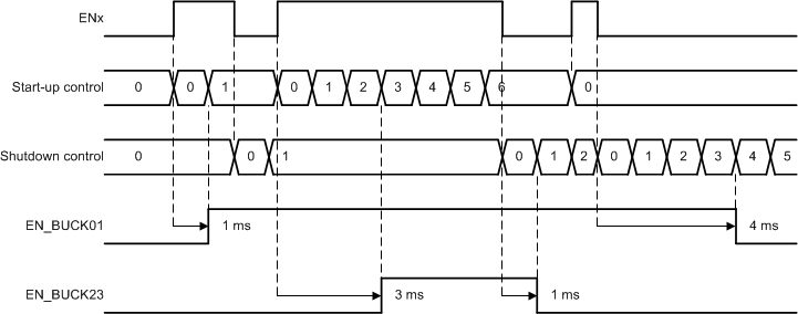
An example of start-up and shutdown sequences is shown in Figure 16 and Figure 17. The start-up and shutdown delays for the BUCK0, BUCK1 regulators are 1 ms and 4 ms and for the BUCK2, BUCK3 regulators 3 ms and 1 ms. The delay settings are used only for enable/disable control with EN1, EN2, EN3 signals, not for Roof/Floor control.
 Figure 16. Typical Start-Up and Shutdown Sequencing
  Figure 17. Start-Up and Shutdown Sequencing With Short ENx Low and High Periods