SNVS296J December 2006 – June 2016 LP3991
PRODUCTION DATA.
- 1 Features
- 2 Applications
- 3 Description
- 4 Revision History
- 5 Pin Configuration and Functions
- 6 Specifications
- 7 Detailed Description
- 8 Application and Implementation
- 9 Power Supply Recommendations
- 10Layout
- 11Device and Documentation Support
- 12Mechanical, Packaging, and Orderable Information
7 Detailed Description
7.1 Overview
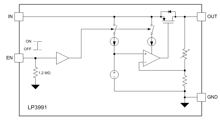
The LP3991 device is a monolithic integrated low-dropout voltage regulator with a low input operating voltage tolerance. Key protection circuits, including output current limitation and thermal shutdown, are integrated in the device. Using the EN pin, the device may be controlled to provide a shutdown state, in which negligible supply current is drawn. The LP3991 is designed to be stable with space-saving ceramic capacitors as small as 0402 case size.
7.2 Functional Block Diagram

7.3 Feature Description
7.3.1 Post-Buck Regulator
Linear post-regulation can be an effective way to reduce ripple and switching noise from DC-DC convertors while still maintaining a reasonably high overall efficiency.
The LP3991 is particularly suitable for this role due to its low input voltage requirements. In addition, there is often no need for a separate input capacitor for the LP3991 as it can share the output cap of the DC-DC convertor.
Care of PCB layouts involving switching regulators is paramount. In particular, the ground paths for the LDO must be routed separately from the switcher ground and star connected close to the battery. Routing of the switch pin of the DC-DC convertor must be kept short to minimize radiated EMI. A low pass filter such as a ferrite bead or common mode choke on the battery input leads can further reduce radiated EMI.
Figure 19 shows a typical example using an LM3673, 350-mA DC-DC buck regulator with a nominal output of 1.8 V and a 1.5-V LP3991 device. The overall efficiency is greater than 70% over the full Li-Ion battery voltage range. Maximum efficiency is achieved by minimizing the difference between VIN and VOUT of the LP3991 device. The LP3991-1.5 remains in regulation down to an input voltage of 1.65 V; thus, in this case, a 1.8-V buck with 5% tolerance is adequate for all conditions of temperature and load.
7.3.2 Maximum Supply Voltage and Thermal Considerations
Maximum recommended input voltage is 3.6 V. The device may be operated at 4-V VIN if proper care is given to the board design in regard to thermal dissipation. As a guide, refer to Table 1 for ambient temperature at two input voltages and two load currents for the example board types.
7.4 Device Functional Modes
7.4.1 Enable Control
The LP3991 features an active high enable (EN) pin, which turns the device on when pulled high. When not enabled the regulator output is off and the device typically consumes 2 nA.
If the application does not require the enable switching feature, the EN pin must be tied to VIN to keep the regulator output permanently on.
To ensure proper operation, the signal source used to drive the EN input must be able to swing above and below the specified turnon/off voltage thresholds listed in Typical Characteristics under VIL and VIH.