SNVS296J December 2006 – June 2016 LP3991
PRODUCTION DATA.
- 1 Features
- 2 Applications
- 3 Description
- 4 Revision History
- 5 Pin Configuration and Functions
- 6 Specifications
- 7 Detailed Description
- 8 Application and Implementation
- 9 Power Supply Recommendations
- 10Layout
- 11Device and Documentation Support
- 12Mechanical, Packaging, and Orderable Information
6 Specifications
6.1 Absolute Maximum Ratings
over operating free-air temperature range (unless otherwise noted)(1)(2)(3)| MIN | MAX | UNIT | ||
|---|---|---|---|---|
| IN, OUT pins, voltage to GND | –0.3 | 6.5 | V | |
| EN pin, voltage to GND | –0.3 | (VIN + 0.3) < 6.5 | V | |
| Junction temperature | 150 | °C | ||
| Continuous power dissipation(4) | Internally Limited | |||
| Storage temperature, Tstg | –65 | 150 | °C | |
(1) Stresses beyond those listed under Absolute Maximum Ratings may cause permanent damage to the device. These are stress ratings only, which do not imply functional operation of the device at these or any other conditions beyond those indicated under Recommended Operating Conditions. Exposure to absolute-maximum-rated conditions for extended periods may affect device reliability.
(2) All voltages are with respect to the potential at the GND pin.
(3) If Military/Aerospace specified devices are required, contact the Texas Instruments Sales Office/ Distributors for availability and specifications.
6.2 ESD Ratings
| VALUE | UNIT | |||
|---|---|---|---|---|
| V(ESD) | Electrostatic discharge | Human-body model (HBM), per ANSI/ESDA/JEDEC JS-001(1) | ±2000 | V |
| Charged-device model (CDM), per JEDEC specification JESD22-C101(2) | ±200 | |||
(1) JEDEC document JEP155 states that 500-V HBM allows safe manufacturing with a standard ESD control process.
(2) JEDEC document JEP157 states that 250-V CDM allows safe manufacturing with a standard ESD control process.
6.3 Recommended Operating Conditions
over operating free-air temperature range (unless otherwise noted)| MIN | NOM | MAX | UNIT | ||
|---|---|---|---|---|---|
| Input voltage | 1.65 | 4 | V | ||
| Recommended load current | 300 | mA | |||
| Junction temperature | –40 | 125 | °C | ||
| Ambient temperature, TA(1) | –40 | 85 | °C | ||
(1) The maximum ambient temperature (TA-MAX) is a suggested value dependant on the maximum operating junction temperature (TJ-MAX-OP) = 125°C); the maximum power dissipation of the device in the application (PD-MAX), and the junction-to-ambient thermal resistance of the part / package in the application (RθJA), as given by the following equation: TA-MAX = TJ-MAX-OP – (RθJA × PD-MAX).
6.4 Thermal Information
| THERMAL METRIC(1) | LP3991 | UNIT | |
|---|---|---|---|
| YZR (DSBGA) | |||
| 4 PINS | |||
| RθJA(2) | Junction-to-ambient thermal resistance, High K | 189.7 | °C/W |
| RθJC(top) | Junction-to-case (top) thermal resistance | 0.5 | °C/W |
| RθJB | Junction-to-board thermal resistance | 112.9 | °C/W |
| ψJT | Junction-to-top characterization parameter | 8.7 | °C/W |
| ψJB | Junction-to-board characterization parameter | 112.8 | °C/W |
(1) For more information about traditional and new thermal metrics, see Semiconductor and IC Package Thermal Metrics.
(2) Thermal resistance value RθJA is based on the EIA/JEDEC High-K printed circuit board defined by: JESD51-7 - High Effective Thermal Conductivity Test Board for Leaded Surface Mount Packages.
6.5 Electrical Characteristics
Unless otherwise noted, VEN = 950 mV, VIN = VOUT + 0.5 V, or 1.8 V, whichever is higher, CIN = 1 µF, COUT = 4.7 µF, IOUT = 1 mA. Typical values and limits apply for TA = 25°C. Minimum and maximum limits apply over the full junction temperature range for operation, −40°C to +125°C, unless otherwise specified. (1)| PARAMETER | TEST CONDITIONS | MIN | TYP | MAX | UNIT | ||
|---|---|---|---|---|---|---|---|
| VIN | Input voltage | See(2) | 1.65 | 3.6 | V | ||
| See(3)(4)(5) | 4 | ||||||
| ΔVOUT | Output voltage tolerance | VIN = VIN(NOM) to 3.6 V ILOAD = 1 to 300 mA |
TJ = 25°C | –1% | 1% | ||
| –3% | 3% | ||||||
| TJ = –25°C to 85°C | –2.5% | 2.5% | |||||
| Line regulation error | VIN = VOUT(NOM) 0.5 V to 3.6 V, IOUT = 1 mA, 0.8 V ≤ VOUT ≤ 2.8 V |
0.05 | 1 | %/V | |||
| Load regulation error | IOUT = 1 mA to 300 mA | 10 | 60 | µV/mA | |||
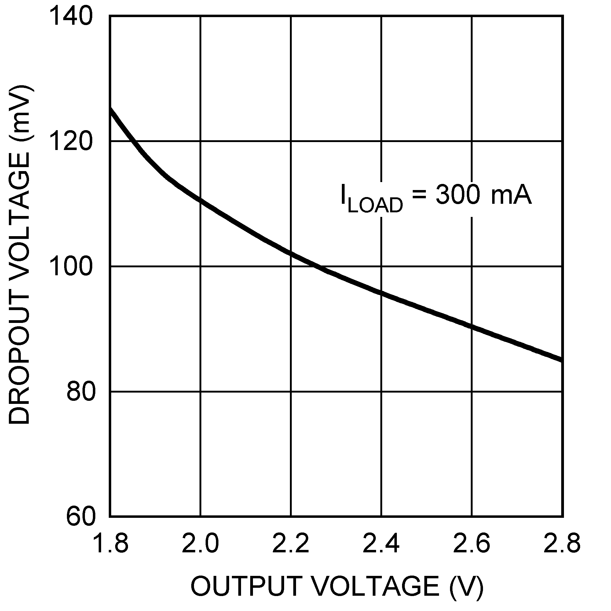
| VDO | Dropout voltage(6) | 1.8 V ≤ VOUT ≤ 2.5 V | IOUT = 150 mA | 55 | 90 | mV | |
| IOUT = 300 mA | 110 | 180 | |||||
| VOUT > 2.5 V | IOUT = 150 mA | 40 | 80 | ||||
| IOUT = 300 mA | 75 | 160 | |||||
| ILOAD | Minimum load current | See(7) | 0 | mA | |||
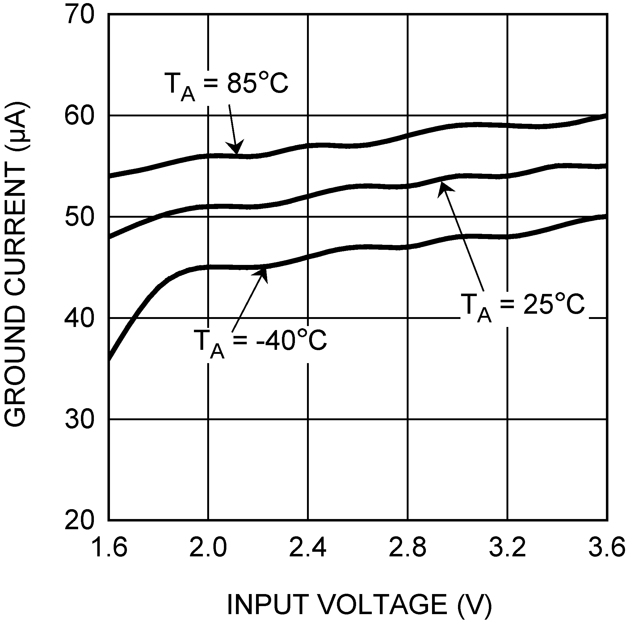
| IQ | Quiescent current | VEN = 950 mV, IOUT = 0 mA | 50 | 100 | µA | ||
| VEN = 950 mV, IOUT = 300 mA | 120 | 225 | |||||
| VEN = 0.4 V | 0.001 | 1 | |||||
| ISC | Short-circuit current limit | VIN = 3.6 V(8) | 550 | 900 | mA | ||
| IOUT | Maximum output current | 300 | mA | ||||
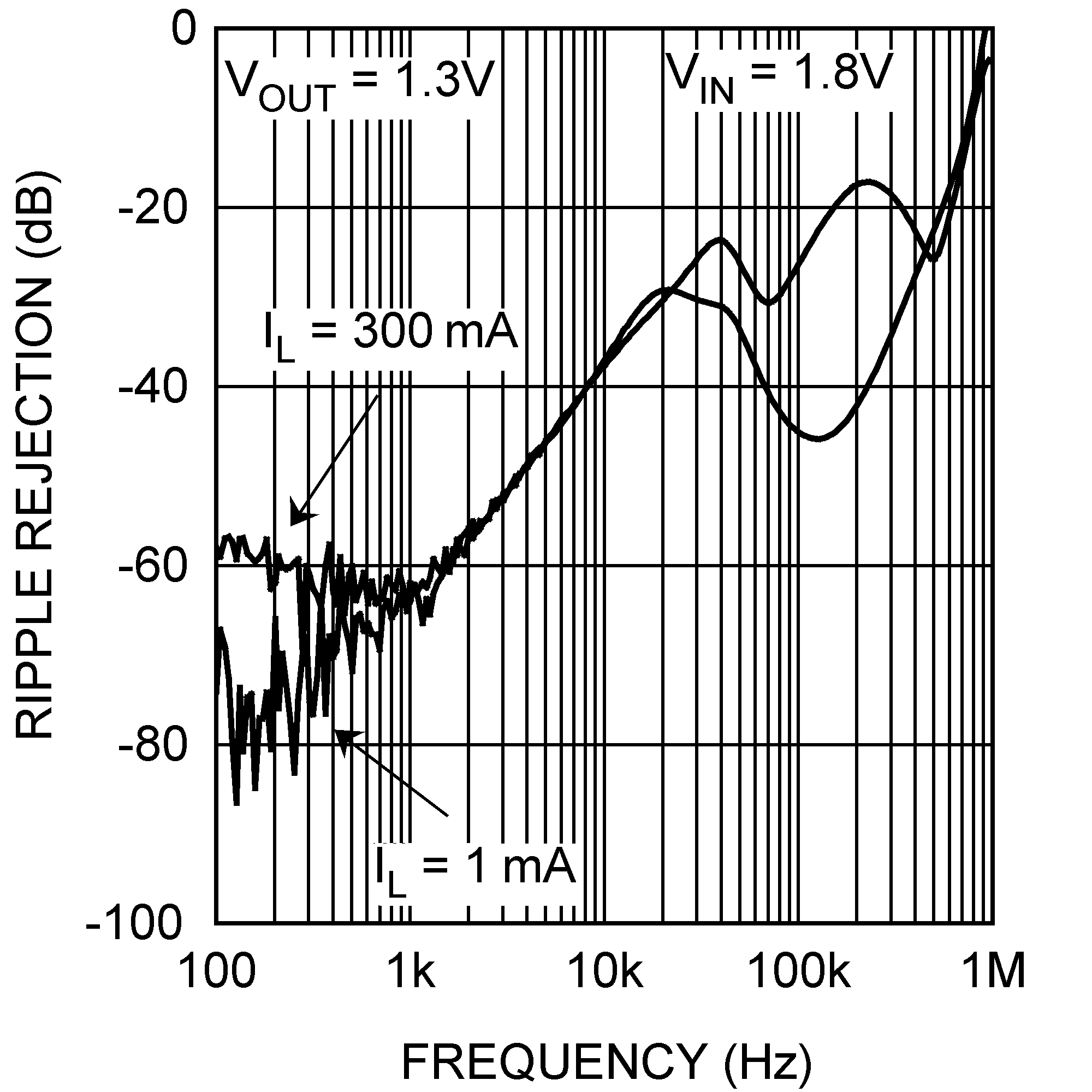
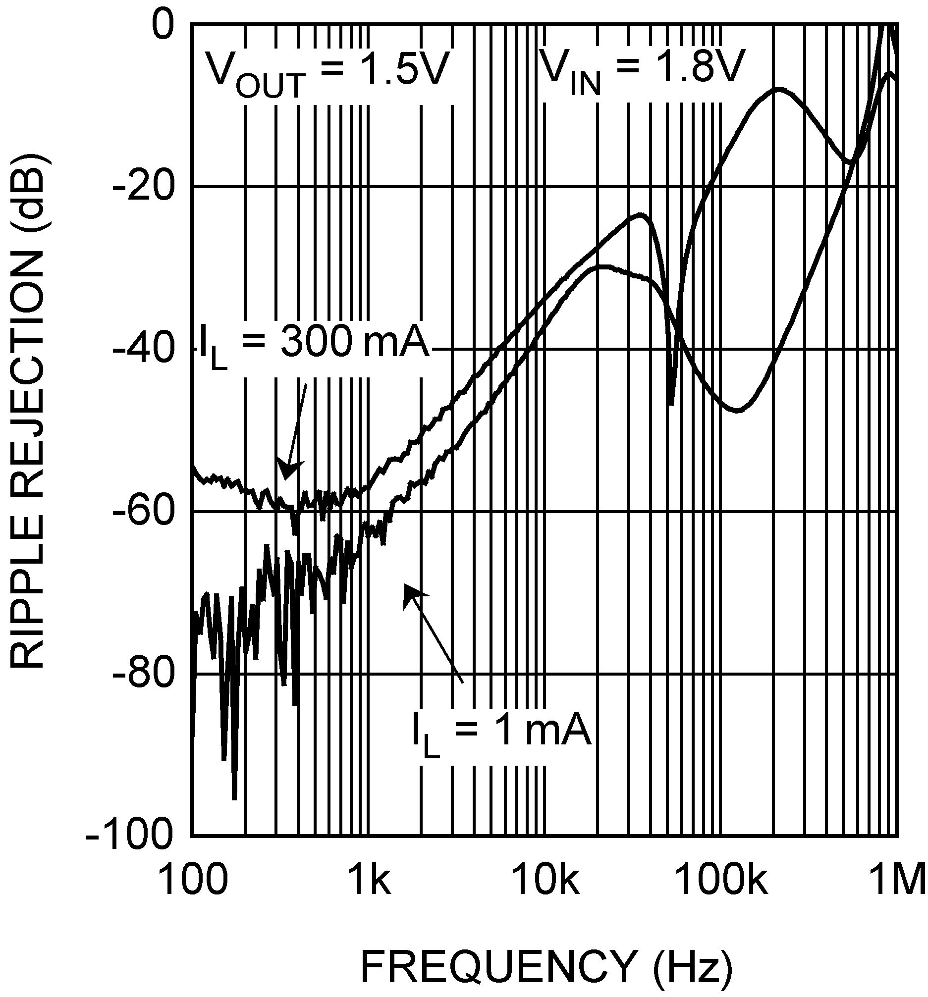
| PSRR | Power Supply Rejection Ratio(9) | ƒ = 1kHz, IOUT = 1 mA to 300 mA | 65 | dB | |||
| en | Output noise voltage(9) | BW = 10 Hz to 100 kHz, VIN = 4.2 V, COUT = 4.7 µF |
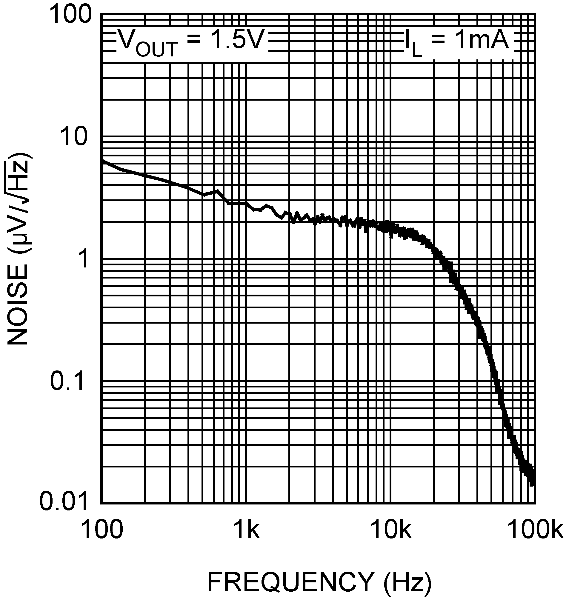
280 | µVRMS | |||
| TSHUTDOWN | Thermal shutdown | Temperature | 160 | °C | |||
| Hysteresis | 20 | ||||||
| ENABLE CONTROL CHARACTERISTICS | |||||||
| IEN(10) | Maximum input current at VEN input | VEN = 0 V, VIN = 3.6 V | 0.001 | µA | |||
| VEN = VIN = 3.6 V | 3 | 5.5 | |||||
| VIL | Low input threshold | VIN = 1.65 V to 3.6 V | 0.4 | V | |||
| VIH | High input threshold | VIN = 1.65 V to 3.6 V | 0.95 | V | |||
| TIMING CHARACTERISTICS | |||||||
| Transient Response | Line transient response |δVOUT| | Trise = Tfall = 30 µs(9)
δVIN = 600 mV |
6 | mV (pk - pk) |
|||
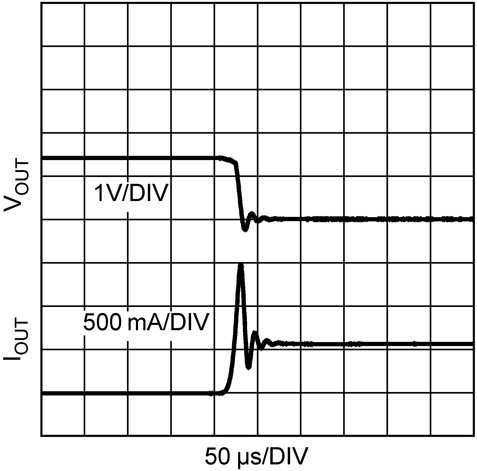
| Load transient response |δVOUT| | Trise = Tfall = 1 µs(9) | IOUT = 0 mA to 300 mA | 140 | mV | |||
| IOUT = 1 mA to 300 mA | 110 | ||||||
| IOUT = 300 mA to 1 mA | 80 | ||||||
| IOUT = 0 mA to 200 mA | 110 | ||||||
| IOUT = 1 mA to 200 mA | 80 | ||||||
| IOUT = 200 mA to 1 mA | 60 | ||||||
| IOUT = 0 mA to 150 mA | 100 | ||||||
| IOUT = 1 mA to 150 mA | 70 | ||||||
| IOUT = 150 mA to 1 mA | 50 | ||||||
| Overshoot on start-up | 0% | 2% | |||||
| IIR | In-rush current(9) | 600 | 1000 | mA | |||
| OUTPUT CAPACITANCE | |||||||
| COUT | Output capacitor | Capacitance(11) | VOUT ≥ 1.5 V | 2 | 4.7 | µF | |
| VOUT < 1.5 V(12) | 1.6 | 2.2 | |||||
| ESR | 5 | 500 | mΩ | ||||
(1) All limits are ensured. All electrical characteristics having room-temperature limits are tested during production at TJ = 25°C or correlated using Statistical Quality Control methods. Operation over the temperature specification is ensured by correlating the electrical characteristics to process and temperature variations and applying statistical process control.
(2) All voltages are with respect to the potential at the GND pin.
(3) VIN(MIN) = VOUT(NOM) + 0.5 V or 1.65 V, whichever is greater. (See Figure 19 in DSBGA Light Sensitivity.)
(4) The device operates with input voltages up to 4 V. However special care must be taken in relation to thermal dissipation and the need to derate the maximum allowable ambient temperature.
(5) The maximum ambient temperature (TA-MAX) is a suggested value dependant on the maximum operating junction temperature (TJ-MAX-OP) = 125°C); the maximum power dissipation of the device in the application (PD-MAX), and the junction-to-ambient thermal resistance of the part / package in the application (RθJA), as given by the following equation: TA-MAX = TJ-MAX-OP – (RθJA × PD-MAX).
(6) Dropout voltage is voltage difference between input and output at which the output voltage drops to 100 mV below its nominal value. This parameter is only specified for output voltages above 1.8 V.
(7) The device maintains the regulated output voltage without a load.
(8) Short circuit current is measured with VOUT pulled to 0 V.
(9) This electrical specification is ensured by design.
(10) EN pin has an internal 1.2-MΩ (typical) resistor connected to GND.
(11) The capacitor tolerance must be 30% or better over temperature. The full operating conditions for the application must be considered when selecting a suitable capacitor to ensure that the minimum value of capacitance is always met. Recommended capacitor type is X7R or X5R. (See External Capacitors in Detailed Design Procedure.)
(12) On lower voltage options, 2.2-µF output capacitor may be used but some degradation in load transient (10 -15%) can be expected, compared to a 4.7-µF capacitor.
6.6 Timing Requirements
| MIN | NOM | MAX | UNIT | ||
|---|---|---|---|---|---|
| tON | Turnon time(1) To 95% Level VIN(MIN) to 3.6 V, VOUT ≤ 2 V |
100 | µs | ||
| Turnon time(1) To 95% Level VIN(MIN) to 3.6 V, VOUT ≥ 2 V |
140 | ||||
(1) This electrical specification is ensured by design.
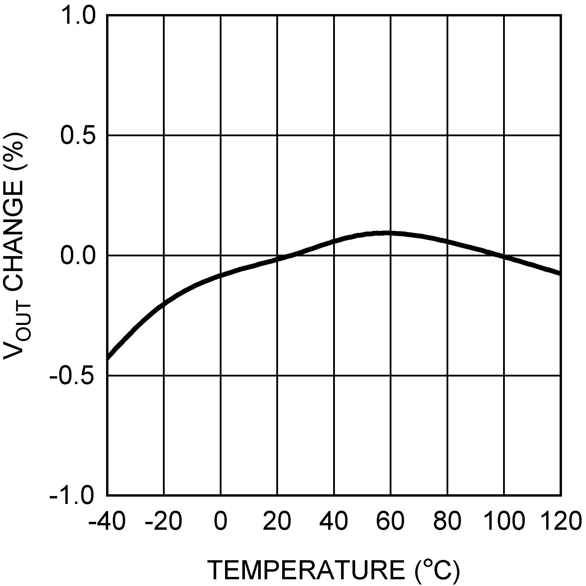
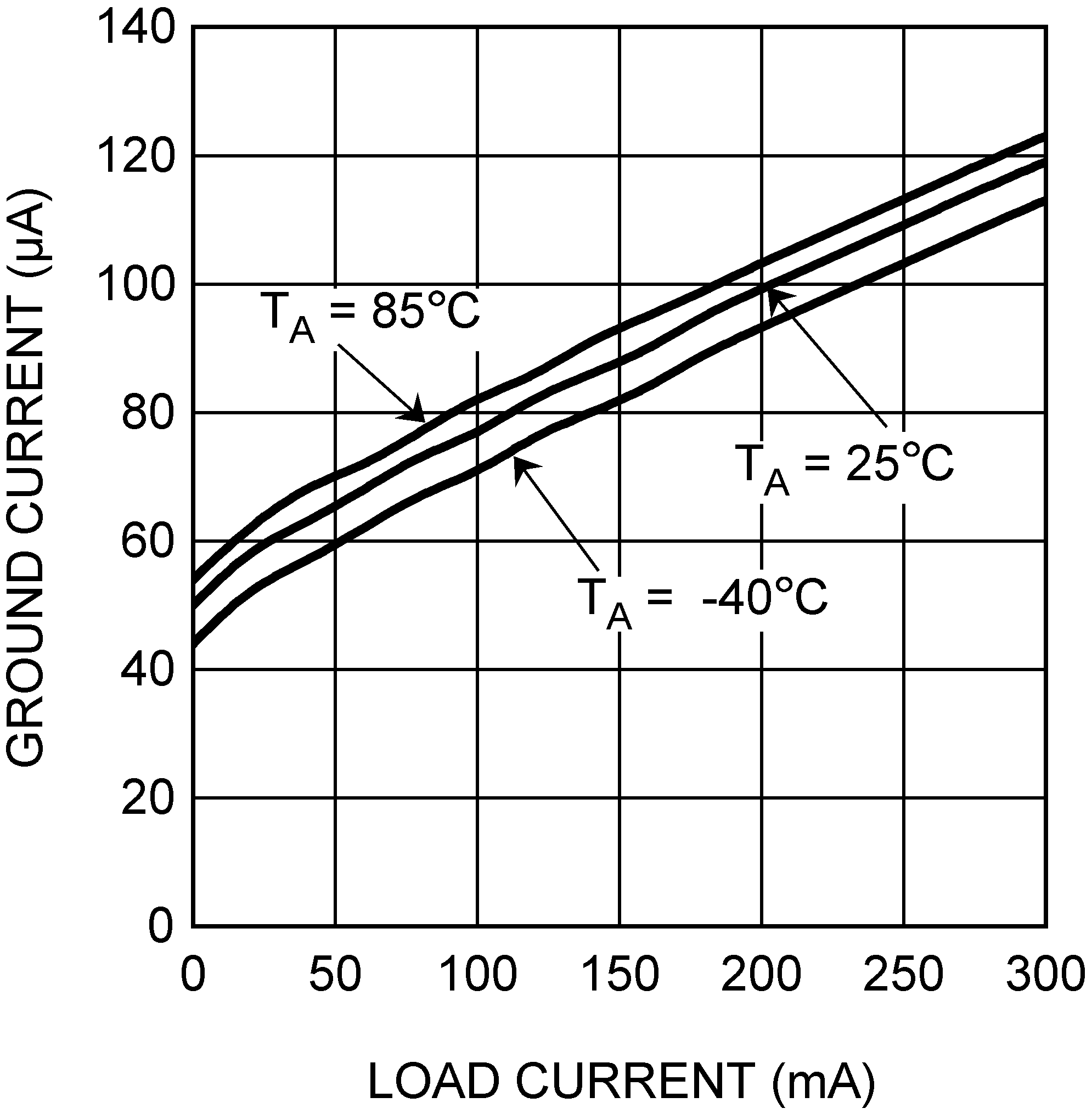
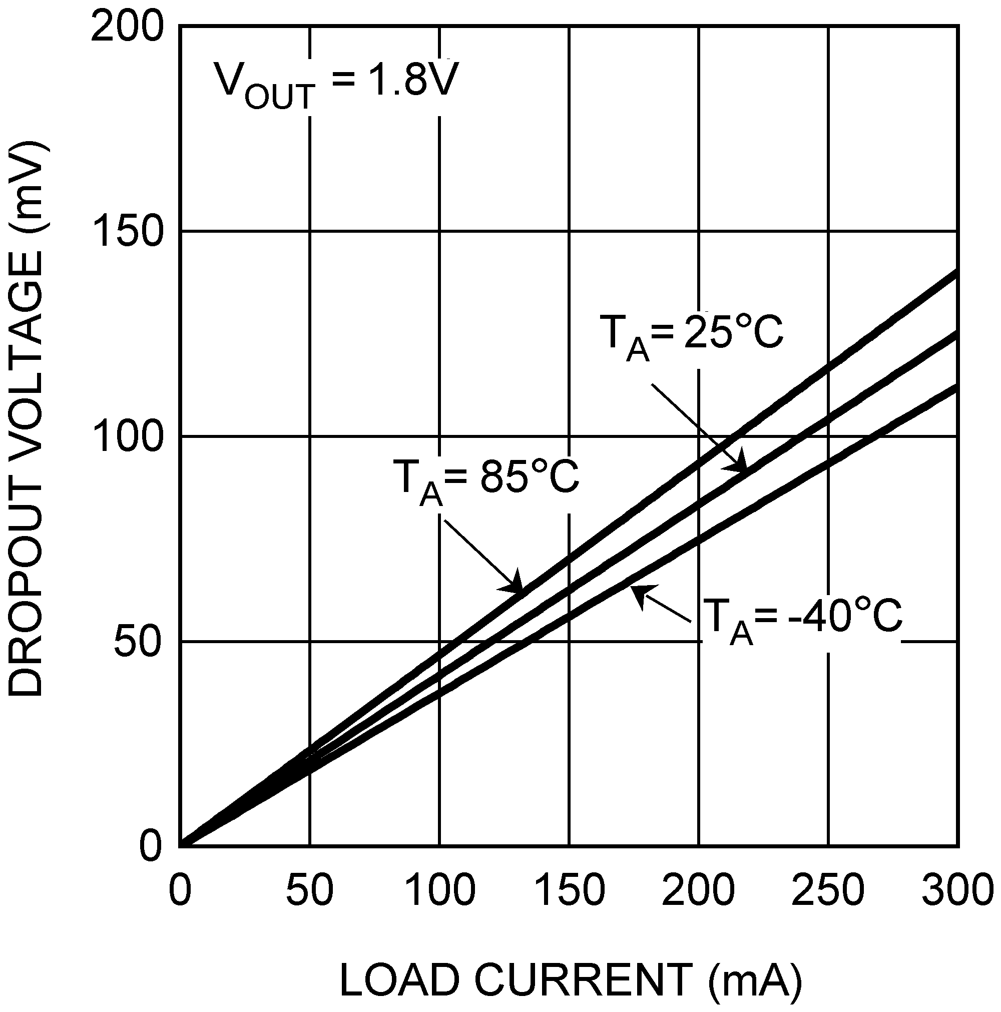
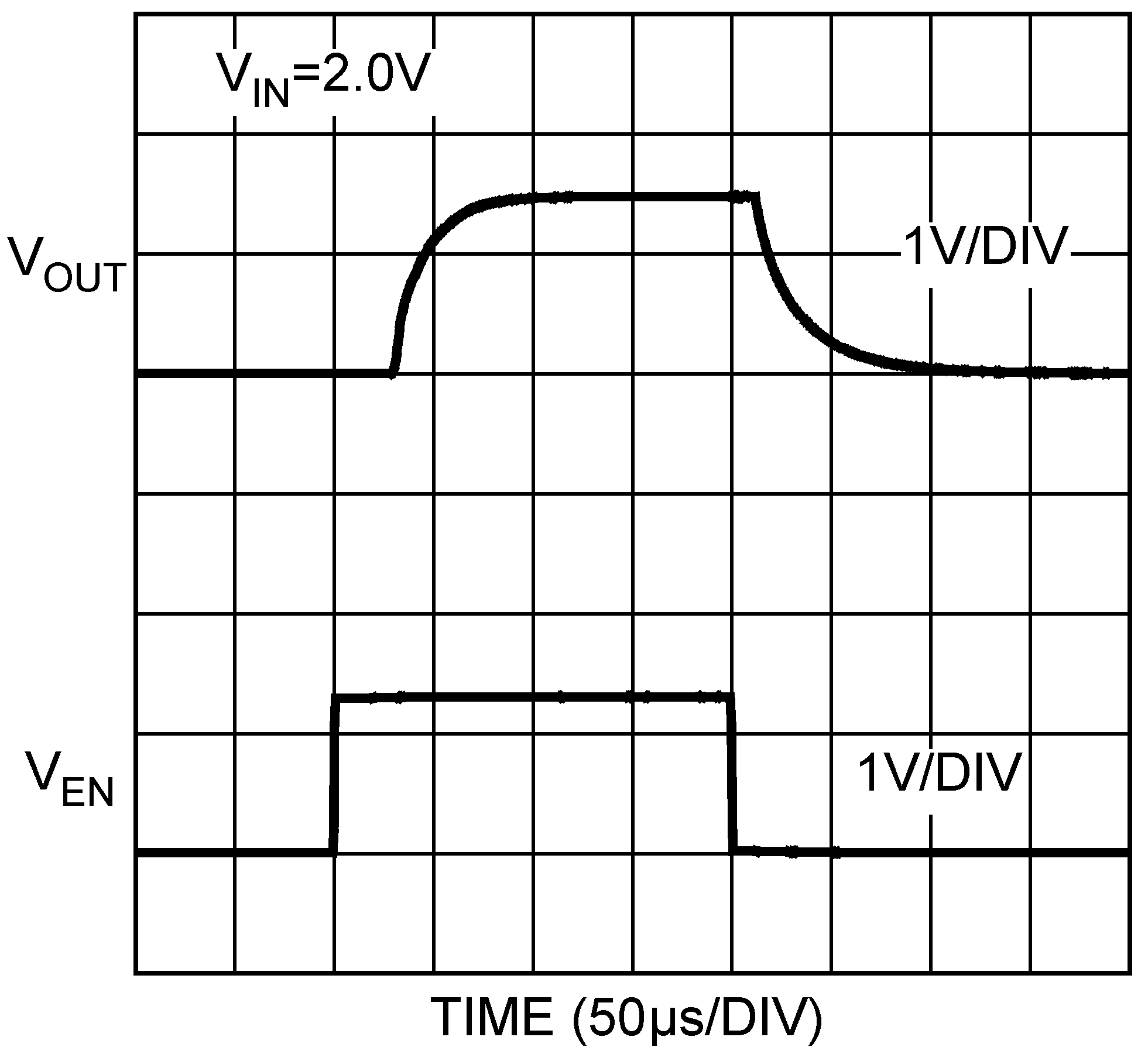
6.7 Typical Characteristics
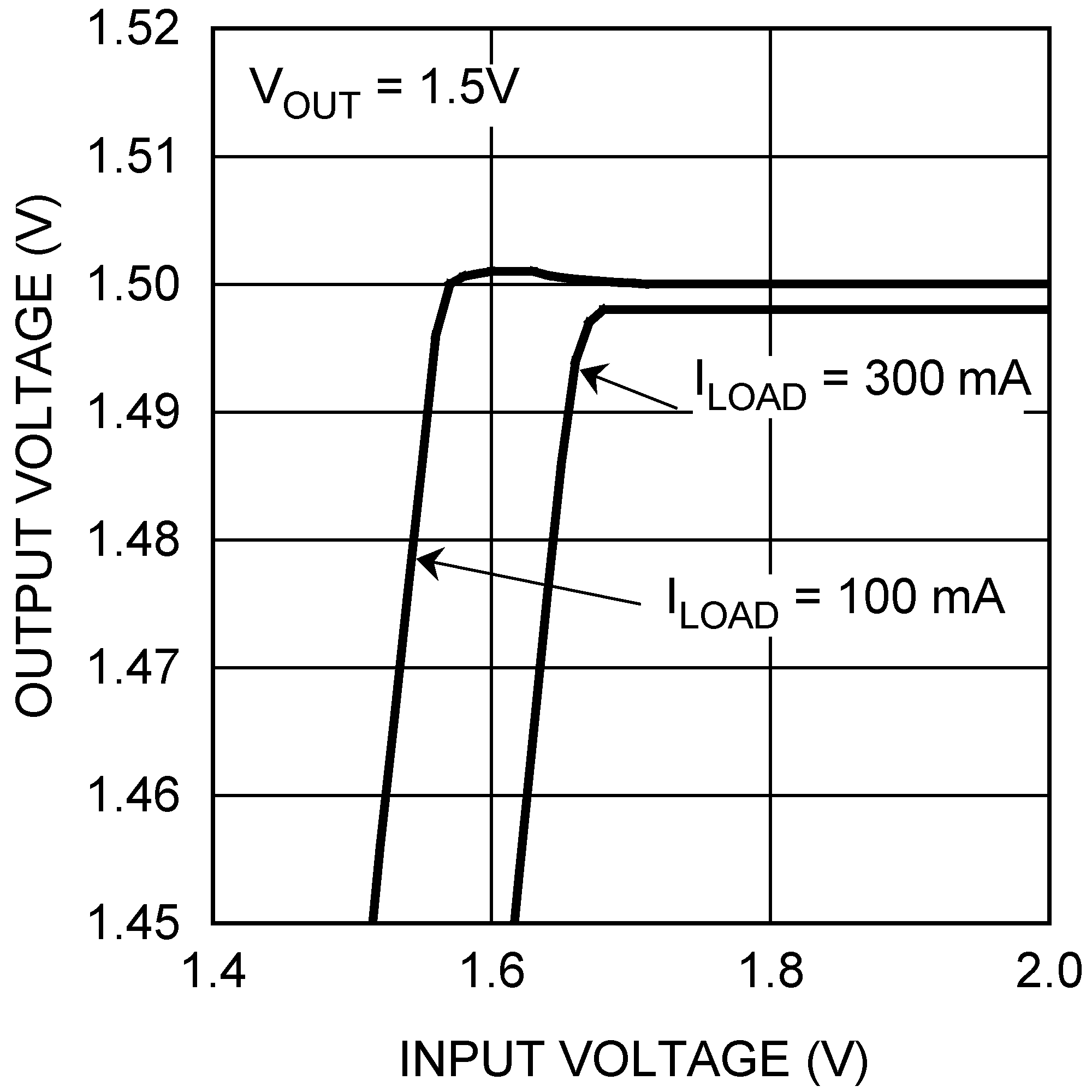
Unless otherwise specified, CIN = 1 µF ceramic, COUT = 4.7 µF ceramic, VIN = VOUT(NOM) + 0.5 V or 1.8 V, whichever is greater, TA = 25°C, VOUT(NOM) = 1.5 V, EN pin is tied to VIN.