SNVS256D Novmeber 2003 – November 2016 LP3943
PRODUCTION DATA.
- 1 Features
- 2 Applications
- 3 Description
- 4 Revision History
- 5 Pin Configuration and Functions
- 6 Specifications
- 7 Detailed Description
- 8 Application and Implementation
- 9 Power Supply Recommendations
- 10Layout
- 11Device and Documentation Support
- 12Mechanical, Packaging, and Orderable Information
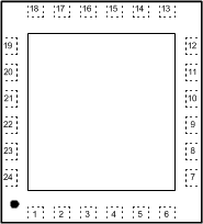
5 Pin Configuration and Functions
RTW Package
24-Pin WQFN With Exposed Pad
Top View

Pin Functions
| PIN | I/O | DESCRIPTION | |
|---|---|---|---|
| NUMBER | NAME | ||
| 1 | LED0 | Output | Output of LED0 Driver |
| 2 | LED1 | Output | Output of LED1 Driver |
| 3 | LED2 | Output | Output of LED2 Driver |
| 4 | LED3 | Output | Output of LED3 Driver |
| 5 | LED4 | Output | Output of LED4 Driver |
| 6 | LED5 | Output | Output of LED5 Driver |
| 7 | LED6 | Output | Output of LED6 Driver |
| 8 | LED7 | Output | Output of LED7 Driver |
| 9 | GND | Ground | Ground |
| 10 | LED8 | Output | Output of LED8 Driver |
| 11 | LED9 | Output | Output of LED9 Driver |
| 12 | LED10 | Output | Output of LED10 Driver |
| 13 | LED11 | Output | Output of LED11 Driver |
| 14 | LED12 | Output | Output of LED12 Driver |
| 15 | LED13 | Output | Output of LED13 Driver |
| 16 | LED14 | Output | Output of LED14 Driver |
| 17 | LED15 | Output | Output of LED15 Driver |
| 18 | RST | Input | Active Low Reset Input |
| 19 | SCL | Input | Clock Line for I2C Interface |
| 20 | SDA | Input/Output | Serial Data Line for I2C Interface |
| 21 | VDD | Power | Power Supply |
| 22 | A0 | Input | Address Input 0 |
| 23 | A1 | Input | Address Input 1 |
| 24 | A2 | Input | Address Input 2 |
| — | Exposed Pad | — | Tie internally to GND pin. |