ZHCSD53F March 2013 – January 2017 LP38798
PRODUCTION DATA.
8 Application and Implementation
NOTE
Information in the following applications sections is not part of the TI component specification, and TI does not warrant its accuracy or completeness. TI’s customers are responsible for determining suitability of components for their purposes. Customers should validate and test their design implementation to confirm system functionality.
8.1 Application Information
The LP38798 is a high-performance linear regulator capable of supplying a well-regulated, low-noise voltage into an 800-mA load. The LP38798 can operate over a wide input voltage range (3 V to 20 V) making it well suited for many post-regulation applications.
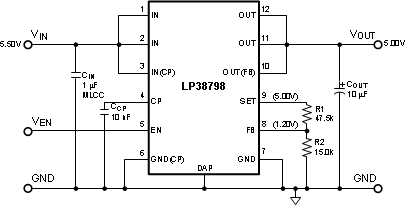
8.2 Typical Application: VOUT = 5 V
 Figure 40. Typical Application, VOUT = 5 V
8.2.1 Design Requirements
| DESIGN PARAMETER | EXAMPLE VALUE |
|---|---|
| Input voltage | 5.5 V, ±10% |
| Output voltage | 5. V, ±3.5% |
| Output current | 500 mA |
8.2.2 Detailed Design Procedure
8.2.2.1 Custom Design With WEBENCH® Tools
Click here to create a custom design using the LP39798 device with the WEBENCH® Power Designer.
- Start by entering the input voltage (VIN), output voltage (VOUT), and output current (IOUT) requirements.
- Optimize the design for key parameters such as efficiency, footprint, and cost using the optimizer dial.
- Compare the generated design with other possible solutions from Texas Instruments.
The WEBENCH Power Designer provides a customized schematic along with a list of materials with real-time pricing and component availability.
In most cases, these actions are available:
- Run electrical simulations to see important waveforms and circuit performance
- Run thermal simulations to understand board thermal performance
- Export customized schematic and layout into popular CAD formats
- Print PDF reports for the design, and share the design with colleagues
Get more information about WEBENCH tools at www.ti.com/WEBENCH.
8.2.2.2 Input Capacitor Recommendations
The LP38798 is designed and characterized for operation with a ceramic capacitor of 1 µF, or greater, at the input. Note especially that the input capacitances must be located as near as practical to the IN pins
The minimum recommended input capacitance is 1 µF, ceramic or tantalum. However, if the LP38798 is operating in conditions where input ripple, fast changes in the input voltage, or large changes in the load current demand are expected, a minimum input capacitance of 10 µF is strongly recommended
Ceramic capacitor tolerance and variations due temperature and applied voltage must be considered when selecting a capacitor to assure the minimum input capacitance requirement is met over the intended operating range.
The input capacitor must be located as close as physically possible to the input pin and returned to a clean analog ground. Any good quality tantalum capacitor may be used, while a ceramic capacitor should be X5R or X7R rated with appropriate adjustments due to the loss of capacitance value from the applied DC voltage.
Attention must be given to the input capacitance value to minimize transient input voltage droop during load current steps at the OUT pin. Larger input capacitor values are necessary for good transient load response, and have no detrimental influence on the stability of the device. Note, however, that using large value ceramic input capacitances can also cause unwanted ringing at the output if the input capacitor, in combination with the trace inductance, creates a high-Q peaking effect during transients. Short, well-designed interconnect leads to the up-stream supply minimize this effect without adding damping. Damping of unwanted ringing can be accomplished by using a tantalum capacitor, with a few hundred milli-ohms of ESR, in parallel with the ceramic input capacitor.
8.2.2.3 Output Capacitor Recommendations
The LP38798 requires an output capacitance of at least 1 µF, ceramic or tantalum; however, a minimum output capacitance of 10 µF is strongly recommended if fast load transient conditions are expected. While the LP38798 is designed to work with Ceramic output capacitors, the output capacitor can be Ceramic, Tantalum, or a combination. The total output capacitance must be sized appropriately to handle any fast load current steps. Capacitance type, tolerance, ESR, as well as temperature and voltage characteristics, must be considered when selecting an output capacitor for the application.
Note especially that the output capacitances must be located as near as practical to the OUT pins.
Even though the LP38798 is stable with an output capacitance of 1 µF to 10 µF, a single output capacitor will generally not be able to provide the best PSRR performance across a wide frequency range. Multiple parallel capacitors, each with a different self-resonance frequency will provide better performance over a wider frequency range.
The LP38798 is characterized with a ceramic capacitor of 10 µF, or greater, at the output. Noise performance is characterized using a single output capacitor of 10 µF ±10%, 16V, X7R, 1206.
8.2.2.4 Charge Pump
The charge pump is running when both the input voltage is above the UVLO threshold (2.65 V typical) and the EN pin voltage is above the VEN(ON) threshold (1.24 V typical). The typical charge pump operating frequency is 3.5 MHz.
A low leakage 10 nF X7R storage capacitor is required between the CP pin and ground to store the energy required for gate drive of the internal NMOS pass device. Larger values of capacitance may slow start-up times, while smaller capacitance values may result in degraded dynamic performance.
Do not make any other connection to the CP pin. Loading this pin in any manner degrades regulator performance. No external biasing may be applied to, or derived from, this pin, as permanent damage to the internal charge pump circuitry may occur.
8.2.2.5 Setting the Output Voltage
The output voltage is buffered from the SET pin. The output voltage is defined as:
Selecting a standard 1% resistor value of 15 kΩ for R2, the resistor value needed for R1 to provide an output voltage of 5V is calculated from:
8.2.2.6 Device Dissipation
Device power dissipation is defined as:
Given 250 mW of device power dissipation, a maximum operating junction temperature (TJ) of 125°C, and presuming a RθJA of 35.4°C/W, the maximum ambient temperature (TA) is defined as:
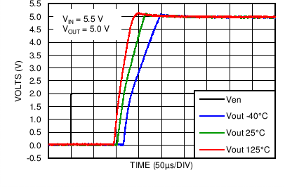
8.2.3 Application Curve
 Figure 41. Start-Up Time