ZHCSD53F March 2013 – January 2017 LP38798
PRODUCTION DATA.
7 Detailed Description
7.1 Overview
The LP38798 is a positive voltage (20 V), ultra-low-noise (5 µVRMS), low-dropout (LDO) regulator capable of supplying a well-regulated, low-noise voltage to an 800-mA load. The LP38798 uses an advanced design with a CMOS process to deliver ultra low output noise and high PSRR at switching power supply (SMPS) frequencies.
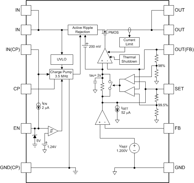
7.2 Functional Block Diagram

7.3 Feature Description
7.3.1 Noise Filter
Any noise at LP38798 SET pin is reduced by an internal passive, first order low-pass RC filter before it is passed to the output buffer stage. The low-pass filter has a –3-dB cut-off frequency of approximately 0.08 Hz.
To keep the low-pass filter from interfering with the output voltage rise time at start-up, a voltage comparator keeps the filter in a fast-charge mode while the output voltage (VOUT) is less than 99.5% of the SET pin voltage (VSET) . When the rising VOUT is within 0.5% of VSET the fast-charge mode ends, and VOUT will rise the final 0.5% based on the RC time constant (τ = 2s) of the filter.
Should VOUT be more than 2% above the VSET voltage, a voltage comparator will put the filter into the fast-charge mode to allow the filter to discharge and VOUT to fall a value closer to VSET. When the falling VOUT is within 2% of VSET the fast-charge mode ends, and VOUT will fall the final 2% based on the RC time constant (τ = 2s) of the filter.
If the input voltage has an extended rise time, the output voltage may exhibit a stair-case waveform as the fast-charge mode is activated and de-activated as VSET rises with VIN, and VOUT follows. Once the VIN has risen above the programmed VSET voltage, and VOUT is within 0.5% of VSET, the stair-case behavior will end.
7.3.2 Enable Input Operation
The Enable pin (EN) is pulled high internally by a 2 μA (typical) current source from the IN pin, and internally clamped at 5 V (typical) by a zener. Pulling the EN pin low, by sinking the IEN current to ground, will turn the output off.
If the EN function is not needed the EN pin should be left open (floating). Do not connect the EN pin directly to VIN if there is any possibility that VIN might exceed 5.5 V (that is, EN pin AbsMax). If external pullup is required, the external current into the EN pin should be limited to no more than 10 μA.
7.3.3 Undervoltage Lockout (UVLO)
The LP38798 incorporates UVLO. The UVLO circuit monitors the input voltage and keeps the LP38798 disabled while a rising VIN is less than 2.65 V (typical). The rising UVLO threshold is approximately 350 mV below the recommended minimum operating VIN of 3 V.
7.3.4 Output Current Limiting
The LP38798 incorporates active output current limiting. The threshold for the output current limiting is set well above the ensured output operating current such that it does not interfere with normal operation.
Note that output current limiting is provided as a safety feature and is outside the recommended operating conditions. Operation at the current limit is not recommended as the device junction temperature (TJ) will rise rapidly and operation will likely cross into thermal shutdown behavior .
7.3.5 Thermal Shutdown
The LP38798 includes thermal protection that will shut-off the output current when activated by excessive device dissipation. Thermal shutdown (TSD) will occur when the junction temperature has risen to 170°C. The junction temperature must fall typically 12°C from the shutdown temperature for the output current to be restored. Junction temperature is calculated from the formula in Equation 2:
Where the power being dissipated, PD, is defined as:
NOTE
Thermal shutdown is provided as a safety feature and is outside the specified Operating Ratings temperature range. Operation with a junction temperature (TJ) above 125°C is not recommended as the device behavior is not specified.
7.4 Device Functional Modes
The LP38798 has two functional modes:
- Enabled: When the EN pin voltage is above the VEN(ON) threshold, and VIN is above the UVLO threshold, the device is enabled.
- Disabled: When the EN pin voltage is below the (VEN(ON) + ΔVEN) threshold, or VIN is below the UVLO threshold, the device is disabled.
7.5 Programming
7.5.1 Programming the Output Voltage
Current sourced from the SET pin, through R1 and R2, must be kept to less than 100 µA. The minimum allowed value for R2 is 12.9 kΩ.
The values for R1 and R2 may be adjusted as needed to achieve the desired output voltage as long as the value for R2 is no less than 12.9 kΩ. The maximum recommended value for R2 is 100 kΩ.
Equation 7 is used to determine the output voltage:
Alternately, Equation 8 can be used to determine the appropriate R1 value for a given R2 value:
Table 1 suggests some ±1% values for R1 and R2 for a range of output voltages using the typical VFB value of 1.200V. This is not a definitive list, as other combinations exist that will provide similar, possibly better, performance.
Table 1. Typical R1 and R2 Values for Assorted Output Voltages
| TARGET VOUT | R1 | R2 | TYPICAL VOUT |
|---|---|---|---|
| 1.2 V | 0 Ω | 15 kΩ | 1.2 V |
| 1.5 V | 4.22 kΩ | 16.9 kΩ | 1.5 V |
| 1.8 V | 10.5 kΩ | 21 kΩ | 1.8 V |
| 2 V | 10 kΩ | 15 kΩ | 2 V |
| 2.5 V | 16.2 kΩ | 15.0 kΩ | 2.496 V |
| 3 V | 21 kΩ | 14 kΩ | 3 V |
| 3.3 V | 23.2 kΩ | 13.3 kΩ | 3.293 V |
| 5 V | 47.5 kΩ | 15 kΩ | 5 V |