SNVS521K December 2007 – August 2014 LP2998 , LP2998-Q1
PRODUCTION DATA.
- 1 Features
- 2 Applications
- 3 Description
- 4 Simplified Schematic
- 5 Revision History
- 6 Pin Configuration and Functions
- 7 Specifications
- 8 Detailed Description
- 9 Application and Implementation
- 10Power Supply Recommendations
- 11Layout
- 12Device and Documentation Support
- 13Mechanical, Packaging, and Orderable Information
封装选项
机械数据 (封装 | 引脚)
散热焊盘机械数据 (封装 | 引脚)
- DDA|8
订购信息
7 Specifications
7.1 Absolute Maximum Ratings (1)(2)
over operating free-air temperature range (unless otherwise noted)| MIN | MAX | UNIT | |
|---|---|---|---|
| AVIN to GND | −0.3 | 6 | V |
| PVIN to GND | –0.3 | AVIN | V |
| VDDQ(3) | −0.3 | 6 | V |
| Junction temperature | 150 | °C | |
| Lead temperature (soldering, 10 sec) | 260 | °C |
(1) Stresses beyond those listed under absolute maximum ratings may cause permanent damage to the device. These are stress ratings only, and functional operation of the device at these or any other conditions beyond those indicated under recommended operating conditions is not implied. Exposure to absolute–maximum–rated conditions for extended periods may affect device reliability.
(2) If Military/Aerospace specified devices are required, please contact the Texas Instruments Sales Office/Distributors for availability and specifications.
(3) VDDQ voltage must be less than 2 x (AVIN - 1) or 6V, whichever is smaller.
7.2 Handling Ratings: LP2998
| MIN | MAX | UNIT | |||
|---|---|---|---|---|---|
| Tstg | Storage temperature range | −65 | 150 | °C | |
| V(ESD) | Electrostatic discharge | Human body model (HBM), per ANSI/ESDA/JEDEC JS-001, all pins(1) | −1000 | 1000 | V |
(1) JEDEC document JEP155 states that 500-V HBM allows safe manufacturing with a standard ESD control process.
7.3 Handling Ratings: LP2998-Q1
| MIN | MAX | UNIT | ||||
|---|---|---|---|---|---|---|
| Tstg | Storage temperature range | −65 | 150 | °C | ||
| V(ESD) | Electrostatic discharge | Human body model (HBM), per AEC Q100-002(1) | −1000 | 1000 | V | |
(1) AEC Q100-002 indicates HBM stressing is done in accordance with the ANSI/ESDA/JEDEC JS-001 specification. The LP2998-Q1 is rated at AEC-Q100 ESD HBM Classification Level H1C.
7.4 Recommended Operating Conditions
over operating free-air temperature range (unless otherwise noted)| MIN | NOM | MAX | UNIT | ||
|---|---|---|---|---|---|
| Junction temperature(1) | –40 | 125 | °C | ||
| AVIN to GND | 2.2 | 5.5 | V | ||
| PVIN supply voltage | 0 | AVIN | V | ||
| SD input voltage | 0 | AVIN | V | ||
7.5 Thermal Information
| THERMAL METRIC(1) | LP2998/LP2998-Q1 | LP2998 | UNIT | |
|---|---|---|---|---|
| SO PowerPAD | SOIC | |||
| 8 PINS | 8 PINS | |||
| RθJA | Junction-to-ambient thermal resistance | 43 | 151 | °C/W |
(1) For more information about traditional and new thermal metrics, see the IC Package Thermal Metrics application report, SPRA953.
7.6 Electrical Characteristics
Typical limits tested at TJ = 25°C. Minimum and maximum limits apply over the full operating junction temperature range (TJ = –40°C to 125°C).(2) Unless otherwise specified, AVIN = PVIN = 2.5 V, VDDQ = 2.5 V.(3)| PARAMETER | TEST CONDITIONS | MIN | TYP | MAX | UNIT | |
|---|---|---|---|---|---|---|
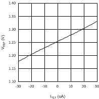
| VREF | VREF voltage (DDR I) | VIN = VDDQ = 2.3 V | 1.135 | 1.158 | 1.185 | V |
| VIN = VDDQ = 2.5 V | 1.235 | 1.258 | 1.285 | |||
| VIN = VDDQ = 2.7 V | 1.335 | 1.358 | 1.385 | |||
| VREF voltage (DDR II) | PVIN = VDDQ = 1.7 V | 0.837 | 0.860 | 0.887 | ||
| PVIN = VDDQ = 1.8 V | 0.887 | 0.910 | 0.937 | |||
| PVIN = VDDQ = 1.9 V | 0.936 | 0.959 | 0.986 | |||
| VREF Voltage (DDR III) | PVIN = VDDQ = 1.35V | 0.669 | 0.684 | 0.699 | ||
| PVIN = VDDQ = 1.5V | 0.743 | 0.758 | 0.773 | |||
| PVIN = VDDQ = 1.6V | 0.793 | 0.808 | 0.823 | |||
| ZVREF | VREF Output Impedance | IREF = –30 to 30 µA | 2.5 | kΩ | ||
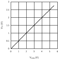
| VTT | VTT Output Voltage (DDR I) (6) | IOUT = 0 A | V | |||
| VIN = VDDQ = 2.3 V | 1.120 | 1.159 | 1.190 | |||
| VIN = VDDQ = 2.5 V | 1.210 | 1.259 | 1.290 | |||
| VIN = VDDQ = 2.7 V | 1.320 | 1.359 | 1.390 | |||
| IOUT = ±1.5 A | ||||||
| VIN = VDDQ = 2.3 V | 1.125 | 1.159 | 1.190 | |||
| VIN = VDDQ = 2.5 V | 1.225 | 1.259 | 1.290 | |||
| VIN = VDDQ = 2.7 V | 1.325 | 1.359 | 1.390 | |||
| VTT Output Voltage (DDR II) (6) | IOUT = 0 A, AVIN = 2.5 V | V | ||||
| PVIN = VDDQ = 1.7 V | 0.822 | 0.856 | 0.887 | |||
| PVIN = VDDQ = 1.8 V | 0.874 | 0.908 | 0.939 | |||
| PVIN = VDDQ = 1.9 V | 0.923 | 0.957 | 0.988 | |||
| IOUT = ±0.5A, AVIN = 2.5 V | ||||||
| PVIN = VDDQ = 1.7 V | 0.820 | 0.856 | 0.890 | |||
| PVIN = VDDQ = 1.8 V | 0.870 | 0.908 | 0.940 | |||
| PVIN = VDDQ = 1.9 V | 0.920 | 0.957 | 0.990 | |||
| VTT Output Voltage (DDR III) (6) | IOUT = 0A, AVIN = 2.5 V | V | ||||
| PVIN = VDDQ = 1.35V | 0.656 | 0.677 | 0.698 | |||
| PVIN = VDDQ = 1.5 V | 0.731 | 0.752 | 0.773 | |||
| PVIN = VDDQ = 1.6 V | 0.781 | 0.802 | 0.823 | |||
| IOUT = 0.2 A, AVIN = 2.5V PVIN = VDDQ = 1.35V |
0.667 | 0.688 | 0.710 | |||
| IOUT = -0.2A, AVIN = 2.5V PVIN = VDDQ = 1.35V |
0.641 | 0.673 | 0.694 | |||
| IOUT = 0.4 A, AVIN = 2.5 V PVIN = VDDQ = 1.5 V |
0.740 | 0.763 | 0.786 | |||
| IOUT = –0.4 A, AVIN = 2.5 V PVIN = VDDQ = 1.5 V |
0.731 | 0.752 | 0.773 | |||
| IOUT = 0.5 A, AVIN = 2.5 V PVIN = VDDQ = 1.6 V |
0.790 | 0.813 | 0.836 | |||
| IOUT = –0.5 A, AVIN = 2.5 V PVIN = VDDQ = 1.6 V |
0.781 | 0.802 | 0.823 | |||
| VOSVtt | VTT Output Voltage Offset (VREF – VTT) for DDR I (6) | IOUT = 0 A | –30 | 0 | 30 | mV |
| IOUT = –1.5 A | –30 | 0 | 30 | |||
| IOUT = 1.5 A | –30 | 0 | 30 | |||
| VTT Output Voltage Offset (VREF – VTT) for DDR II (6) | IOUT = 0 A | –30 | 0 | 30 | ||
| IOUT = –0.5 A | –30 | 0 | 30 | |||
| IOUT = 0.5 A | –30 | 0 | 30 | |||
| VTT Output Voltage Offset (VREF – VTT) for DDR III (6) | IOUT = 0 A | –30 | 0 | 30 | ||
| IOUT = ±0.2 A | –30 | 0 | 30 | |||
| IOUT = ±0.4 A | –30 | 0 | 30 | |||
| IOUT = ±0.5 A | –30 | 0 | 30 | |||
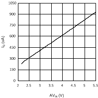
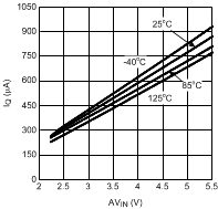
| IQ | Quiescent Current (4) | IOUT = 0 A | 320 | 500 | µA | |
| ZVDDQ | VDDQ Input Impedance | 100 | kΩ | |||
| ISD | Quiescent current in shutdown (4) | SD = 0 V | 115 | 150 | µA | |
| IQ_SD | Shutdown leakage current | SD = 0 V | 2 | 5 | ||
| VIH | Minimum Shutdown High Level | 1.9 | V | |||
| VIL | Maximum Shutdown Low Level | 0.8 | ||||
| Iv | VTT leakage current in shutdown | SD = 0 V VTT = 1.25 V |
1 | 10 | µA | |
| ISENSE | VSENSE Input current | 13 | nA | |||
| TSD | Thermal Shutdown (5) | 165 | °C | |||
| TSD_HYS | Thermal Shutdown Hysteresis | 10 | ||||
(1) At elevated temperatures, devices must be derated based on thermal resistance.
(2) Limits are 100% production tested at 25°C. Limits over the operating temperature range are specified through correlation using Statistical Quality Control (SQC) methods. The limits are used to calculate Texas Instruments' Average Outgoing Quality Level (AOQL).
(3) VIN is defined as VIN = AVIN = PVIN.
(4) Quiescent current defined as the current flow into AVIN.
(5) The maximum allowable power dissipation is a function of the maximum junction temperature, TJ(MAX), the junction to ambient thermal resistance, RθJA, and the ambient temperature, TA. Exceeding the maximum allowable power dissipation will cause excessive die temperature and the regulator will go into thermal shutdown.
(6) VTT load regulation is tested by using a 10 ms current pulse and measuring VTT.
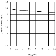
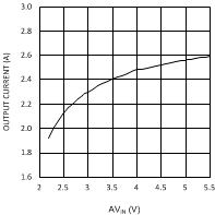
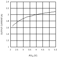
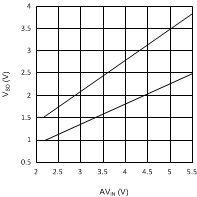
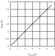
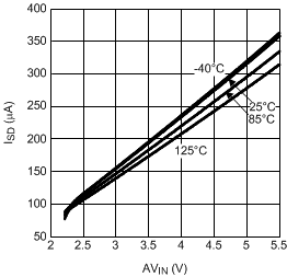
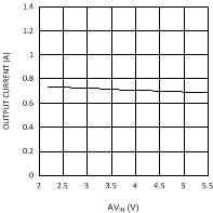
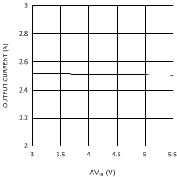
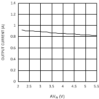
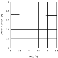
7.7 Typical Characteristics
Unless otherwise specified AVIN = PVIN = 2.5 V.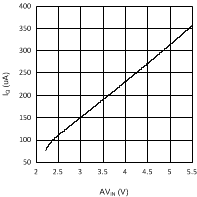
| VDDQ = 2.5 V | PVIN = 1.8 V | |
| VDDQ = 2.5 V | PVIN = 3.3 V | |
| VDDQ = 1.8 V | PVIN = 1.8 V | |
| VDDQ = 1.8 V | PVIN = 3.3 V | |||