SNVS692G January 2011 – October 2015 LMZ14203H
PRODUCTION DATA.
- 1 Features
- 2 Applications
- 3 Description
- 4 Revision History
- 5 Pin Configuration and Functions
- 6 Specifications
- 7 Detailed Description
-
8 Application and Implementation
- 8.1 Application Information
- 8.2
Typical Application
- 8.2.1 Design Requirements
- 8.2.2
Detailed Design Procedure
- 8.2.2.1 Design Steps for the LMZ14203H Application
- 8.2.3 Application Curve
- 9 Power Supply Recommendations
- 10Layout
- 11Device and Documentation Support
- 12Mechanical, Packaging, and Orderable Information
6 Specifications
6.1 Absolute Maximum Ratings(2)(1)(3)
| MIN | MAX | UNIT | |
|---|---|---|---|
| VIN, RON to GND | –0.3 | 43.5 | V |
| EN, FB, SS to GND | –0.3 | 7 | V |
| Junction Temperature | 150 | °C | |
| Peak Reflow Case Temperature (30 s) | 245 | °C | |
| Storage Temperature | –65 | 150 | °C |
(1) Stresses beyond those listed under Absolute Maximum Ratings may cause permanent damage to the device. These are stress ratings only, which do not imply functional operation of the device at these or any other conditions beyond those indicated under Recommended Operating Conditions. Exposure to absolute-maximum-rated conditions for extended periods may affect device reliability.
(2) If Military/Aerospace specified devices are required, please contact the Texas Instruments Sales Office/ Distributors for availability and specifications.
(3) For soldering specifications, see the application note Absolute Maximum Ratings for Soldering (SNOA549)
6.2 ESD Ratings
| VALUE | UNIT | |||
|---|---|---|---|---|
| V(ESD) | Electrostatic discharge | Human body model (HBM), per ANSI/ESDA/JEDEC JS-001(1) | ±2000 | V |
(1) JEDEC document JEP155 states that 500-V HBM allows safe manufacturing with a standard ESD control process.
6.3 Recommended Operating Conditions
| MIN | MAX | UNIT | |
|---|---|---|---|
| VIN | 6 | 42 | V |
| EN | 0 | 6.5 | V |
| Operation Junction Temperature | −40 | 125 | °C |
6.4 Thermal Information
| THERMAL METRIC(1) | LMZ14203H | UNIT | ||
|---|---|---|---|---|
| NDW (TO-PMOD) | ||||
| 7 PINS | ||||
| RθJA | Junction-to-ambient thermal resistance | 4 layer printed-circuit-board, 7.62 cm x 7.62 cm (3 in x 3 in) area, 1-oz copper, no air flow | 16 | °C/W |
| 4 layer printed-circuit-board, 6.35 cm x 6.35 cm (2.5 in x 2.5 in) area, 1-oz copper, no air flow | 18.4 | |||
| RθJC(top) | Junction-to-case (top) thermal resistance | 1.9 | °C/W | |
(1) For more information about traditional and new thermal metrics, see the Semiconductor and IC Package Thermal Metrics application report, SPRA953.
6.5 Electrical Characteristics
Minimum and Maximum limits are ensured through test, design or statistical correlation. Typical values represent the most likely parametric norm at TJ = 25°C, and are provided for reference purposes only. Unless otherwise stated the following conditions apply: VIN = 24 V, VOUT = 12 V, RON = 249 kΩ| PARAMETER | TEST CONDITIONS | MIN(1) | TYP(2) | MAX(1) | UNIT | |
|---|---|---|---|---|---|---|
| SYSTEM PARAMETERS | ||||||
| ENABLE CONTROL | ||||||
| VEN | EN threshold trip point | VEN rising, TJ = –40°C to 125°C | 1.10 | 1.18 | 1.25 | V |
| VEN-HYS | EN threshold hysteresis | 90 | mV | |||
| SOFT-START | ||||||
| ISS | SS source current | VSS = 0 V, TJ = –40°C to 125°C | 8 | 10 | 15 | µA |
| ISS-DIS | SS discharge current | –200 | µA | |||
| CURRENT LIMIT | ||||||
| ICL | Current limit threshold | DC average, TJ = –40°C to 125°C | 3.2 | 4.7 | 5.5 | A |
| VIN UVLO | ||||||
| VINUVLO | Input UVLO | EN pin floating VIN rising |
3.75 | V | ||
| VINUVLO-HYST | Hysteresis | EN pin floating VIN falling |
130 | mV | ||
| ON/OFF TIMER | ||||||
| tON-MIN | ON timer minimum pulse width | 150 | ns | |||
| tOFF | OFF timer pulse width | 260 | ns | |||
| REGULATION AND OVERVOLTAGE COMPARATOR | ||||||
| VFB | In-regulation feedback voltage | VIN = 24 V, VOUT = 12 V VSS >+ 0.8 V TJ = –40°C to 125°C IOUT = 10 mA to 3 A |
0.782 | 0.803 | 0.822 | V |
| VIN = 24 V, VOUT = 12 V VSS >+ 0.8 V TJ = 25°C IOUT = 10 mA to 3 A |
0.786 | 0.803 | 0.818 | |||
| VFB | In-regulation feedback voltage | VIN = 36 V, VOUT = 24 V VSS >+ 0.8 V TJ = –40°C to 125°C IOUT = 10 mA to 3 A |
0.780 | 0.803 | 0.826 | V |
| VIN = 36 V, VOUT = 24 V VSS >+ 0.8 V TJ = 25°C IOUT = 10 mA to 3 A |
0.787 | 0.803 | 0.819 | |||
| VFB-OVP | Feedback overvoltage protection threshold | 0.92 | V | |||
| IFB | Feedback input bias current | 5 | nA | |||
| IQ | Nonswitching Input Current | VFB= 0.86 V | 1 | mA | ||
| ISD | Shutdown quiescent current | VEN= 0 V | 25 | μA | ||
| THERMAL CHARACTERISTICS | ||||||
| TSD | Thermal shutdown (rising) | 165 | °C | |||
| TSD-HYST | Thermal shutdown hysteresis | 15 | °C | |||
| PERFORMANCE PARAMETERS | ||||||
| ΔVOUT | Output Voltage Ripple | VOUT = 5 V, CO = 100-µF 6.3-V X7R | 8 | mV PP | ||
| ΔVOUT/ΔVIN | Line Regulation | VIN = 16 V to 42 V, IOUT= 3 A | 0.01% | |||
| ΔVOUT/ΔIOUT | Load Regulation | VIN = 24 V, IOUT = 0 A to 3 A | 1.5 | mV/A | ||
| η | Efficiency | VIN = 24 V, VOUT = 12 V, IOUT = 1 A | 94% | |||
| η | Efficiency | VIN = 24 V, VO = 12 V, IO = 3 A | 93% | |||
(1) Minimum and Maximum limits are 100% production tested at 25°C. Limits over the operating temperature range are ensured through correlation using Statistical Quality Control (SQC) methods. Limits are used to calculate National’s Average Outgoing Quality Level (AOQL).
(2) Typical numbers are at 25°C and represent the most likely parametric norm.
6.6 Typical Characteristics
Unless otherwise specified, the following conditions apply: VIN = 24 V; Cin = 10-uF X7R Ceramic; CO = 47 uF; TA = 25°C.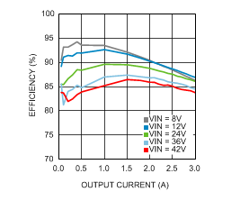 Figure 1. Efficiency VOUT = 5 V, TA = 25°C
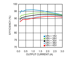 Figure 3. Efficiency VOUT = 12 V, TA = 25°C
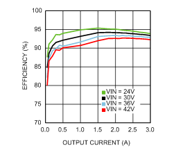 Figure 5. Efficiency VOUT = 15 V, TA = 25°C
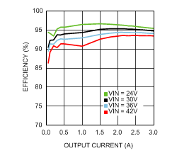 Figure 7. Efficiency VOUT = 18 V, TA = 25°C
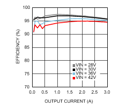 Figure 9. Efficiency VOUT = 24 V, TA = 25°C
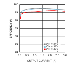 Figure 11. Efficiency VOUT = 30 V, TA = 25°C
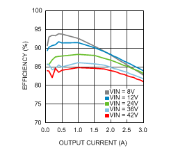 Figure 13. Efficiency VOUT = 5 V, TA = 85°C
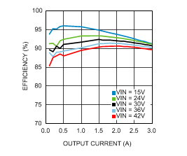 Figure 15. Efficiency VOUT = 12 V, TA = 85°C
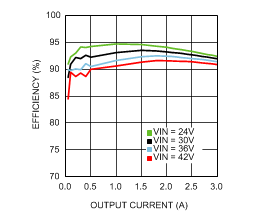 Figure 17. Efficiency VOUT = 15 V, TA = 85°C
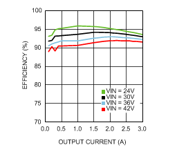 Figure 19. Efficiency VOUT = 18 V, TA = 85°C
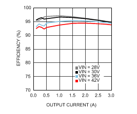 Figure 21. Efficiency VOUT = 24 V, TA = 85°C
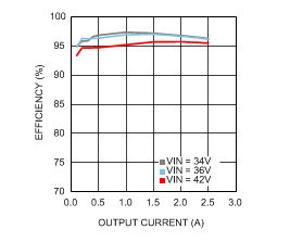 Figure 23. Efficiency VOUT = 30 V, TA = 85°C
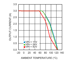 Figure 25. Thermal Derating VOUT = 12 V, RθJA = 16°C/W
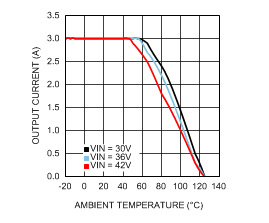 Figure 27. Thermal Derating VOUT = 24 V, RθJA = 16°C/W
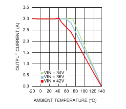 Figure 29. Thermal Derating VOUT = 30 V, RθJA = 16°C/W
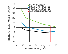 Figure 31. Package Thermal Resistance RθJA
4-Layer Printed-Circuit-Board With 1-oz Copper
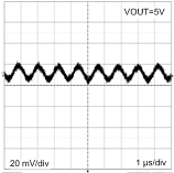 Figure 33. Output Ripple
VIN = 12 V, IOUT = 3 A, Ceramic COUT, BW = 200 MHz
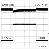 Figure 35. Load Transient Response VIN = 24 V, VOUT = 12 V
Load Step From 10% to 100%
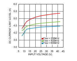 Figure 37. Current Limit vs Input Voltage
VOUT = 5 V
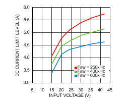 Figure 39. Current Limit vs Input Voltage
VOUT = 12 V
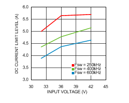 Figure 41. Current Limit vs Input Voltage
VOUT = 24 V
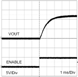
VIN = 24 V, IOUT = 3 A
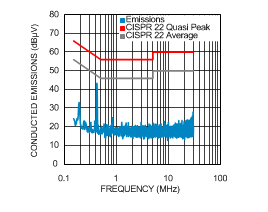 Figure 45. Conducted EMI, VOUT = 12 V
Evaluation Board BOM and 3.3 µH 2x10 µF LC Line Filter
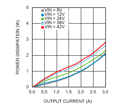 Figure 2. Power Dissipation VOUT = 5 V, TA = 25°C
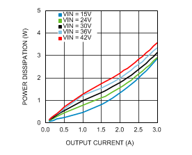 Figure 4. Power Dissipation VOUT = 12 V, TA = 25°C
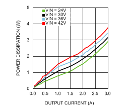 Figure 6. Power Dissipation VOUT = 15 V, TA = 25°C
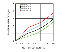 Figure 8. Power Dissipation VOUT = 18 V, TA = 25°C
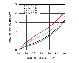 Figure 10. Power Dissipation VOUT = 24 V, TA = 25°C
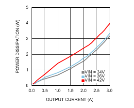 Figure 12. Power Dissipation VOUT = 30 V, TA = 25°C
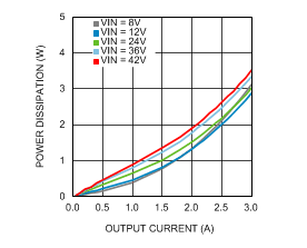 Figure 14. Power Dissipation VOUT = 5 V, TA = 85°C
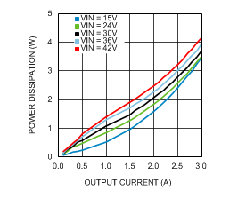 Figure 16. Power Dissipation VOUT = 12 V, TA = 85°C
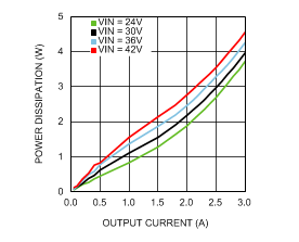 Figure 18. Power Dissipation VOUT = 15 V, TA = 85°C
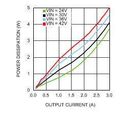 Figure 20. Power Dissipation VOUT = 18 V, TA = 85°C
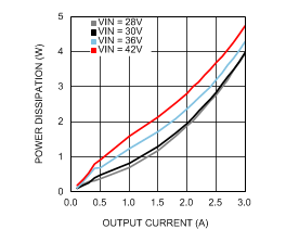 Figure 22. Power Dissipation VOUT = 24 V, TA = 85°C
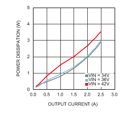 Figure 24. Power Dissipation VOUT = 30 V, TA = 85°C
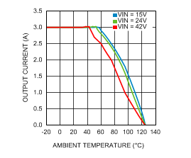 Figure 26. Thermal Derating VOUT = 12 V, RθJA = 20°C/W
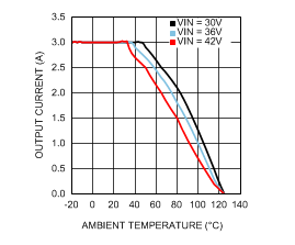 Figure 28. Thermal Derating VOUT = 24 V, RθJA = 20°C/W
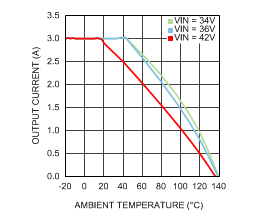 Figure 30. Thermal Derating VOUT = 30 V, RθJA = 20°C/W
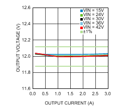 Figure 32. Line and Load Regulation TA = 25°C
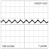 Figure 34. Output Ripple
VIN = 24 V, IOUT = 3 A, Polymer Electrolytic COUT, BW = 200 MHz
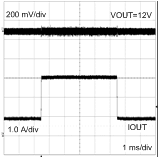 Figure 36. Load Transient Response VIN = 24 V, VOUT = 12 V
Load Step From 30% to 100%
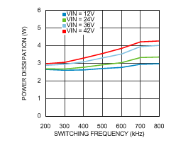 Figure 38. Switching Frequency vs Power Dissipation
VOUT = 5 V
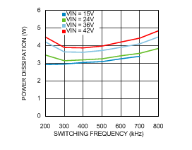 Figure 40. Switching Frequency vs Power Dissipation
VOUT = 12 V
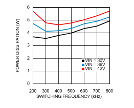 Figure 42. Switching Frequency vs Power Dissipation
VOUT = 24 V
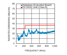 Figure 44. Radiated EMI of Evaluation Board, VOUT = 12 V