ZHCSGL4C June   2017  – April 2019 LMX2595

PRODUCTION DATA.  

  1. 特性
  2. 应用
  3. 说明
    1.     Device Images
      1.      简化原理图
  4. 修订历史记录
  5. Pin Configuration and Functions
    1.     Pin Functions
  6. Specifications
    1. 6.1 Absolute Maximum Ratings
    2. 6.2 ESD Ratings
    3. 6.3 Recommended Operating Conditions
    4. 6.4 Thermal Information
    5. 6.5 Electrical Characteristics
    6. 6.6 Timing Requirements
    7. 6.7 Typical Characteristics
  7. Detailed Description
    1. 7.1 Overview
    2. 7.2 Functional Block Diagram
    3. 7.3 Feature Description
      1. 7.3.1  Reference Oscillator Input
      2. 7.3.2  Reference Path
        1. 7.3.2.1 OSCin Doubler (OSC_2X)
        2. 7.3.2.2 Pre-R Divider (PLL_R_PRE)
        3. 7.3.2.3 Programmable Multiplier (MULT)
        4. 7.3.2.4 Post-R Divider (PLL_R)
        5. 7.3.2.5 State Machine Clock
      3. 7.3.3  PLL Phase Detector and Charge Pump
      4. 7.3.4  N-Divider and Fractional Circuitry
      5. 7.3.5  MUXout Pin
        1. 7.3.5.1 Lock Detect
        2. 7.3.5.2 Readback
      6. 7.3.6  VCO (Voltage-Controlled Oscillator)
        1. 7.3.6.1 VCO Calibration
        2. 7.3.6.2 Determining the VCO Gain
      7. 7.3.7  Channel Divider
      8. 7.3.8  VCO Doubler
      9. 7.3.9  Output Buffer
      10. 7.3.10 Power-Down Modes
      11. 7.3.11 Phase Synchronization
        1. 7.3.11.1 General Concept
        2. 7.3.11.2 Categories of Applications for SYNC
        3. 7.3.11.3 Procedure for Using SYNC
        4. 7.3.11.4 SYNC Input Pin
      12. 7.3.12 Phase Adjust
      13. 7.3.13 Fine Adjustments for Phase Adjust and Phase SYNC
      14. 7.3.14 Ramping Function
        1. 7.3.14.1 Manual Pin Ramping
          1. 7.3.14.1.1 Manual Pin Ramping Example
        2. 7.3.14.2 Automatic Ramping
          1. 7.3.14.2.1 Automatic Ramping Example (Triangle Wave)
      15. 7.3.15 SYSREF
        1. 7.3.15.1 Programmable Fields
        2. 7.3.15.2 Input and Output Pin Formats
          1. 7.3.15.2.1 Input Format for SYNC and SysRefReq Pins
          2. 7.3.15.2.2 SYSREF Output Format
        3. 7.3.15.3 Examples
        4. 7.3.15.4 SYSREF Procedure
      16. 7.3.16 SysRefReq Pin
    4. 7.4 Device Functional Modes
    5. 7.5 Programming
      1. 7.5.1 Recommended Initial Power-Up Sequence
      2. 7.5.2 Recommended Sequence for Changing Frequencies
      3. 7.5.3 General Programming Requirements
    6. 7.6 Register Maps
      1. 7.6.1  General Registers R0, R1, & R7
        1. Table 25. Field Descriptions
      2. 7.6.2  Input Path Registers
        1. Table 26. Field Descriptions
      3. 7.6.3  Charge Pump Registers (R13, R14)
        1. Table 27. Field Descriptions
      4. 7.6.4  VCO Calibration Registers
        1. Table 28. Field Descriptions
      5. 7.6.5  N Divider, MASH, and Output Registers
        1. Table 29. Field Descriptions
      6. 7.6.6  SYNC and SysRefReq Input Pin Register
        1. Table 30. Field Descriptions
      7. 7.6.7  Lock Detect Registers
        1. Table 31. Field Descriptions
      8. 7.6.8  MASH_RESET
        1. Table 32. Field Descriptions
      9. 7.6.9  SysREF Registers
        1. Table 33. Field Descriptions
      10. 7.6.10 CHANNEL Divider And VCO Doubler Registers
        1. Table 34. Field Descriptions
      11. 7.6.11 Ramping and Calibration Fields
        1. Table 35. Field Descriptions
      12. 7.6.12 Ramping Registers
        1. 7.6.12.1 Ramp Limits
          1. Table 36. Field Descriptions
        2. 7.6.12.2 Ramping Triggers, Burst Mode, and RAMP0_RST
          1. Table 37. Field Descriptions
        3. 7.6.12.3 Ramping Configuration
          1. Table 38. Field Descriptions
      13. 7.6.13 Readback Registers
        1. Table 39. Field Descriptions
  8. Application and Implementation
    1. 8.1 Application Information
      1. 8.1.1 OSCin Configuration
      2. 8.1.2 OSCin Slew Rate
      3. 8.1.3 RF Output Buffer Power Control
      4. 8.1.4 RF Output Buffer Pullup
      5. 8.1.5 Performance Comparison Between 1572 (0x0624) and 3115 (0x0C2B) for Register DBLR_IBIAS_CTRL1 (R25[15:0])
    2. 8.2 Typical Application
      1. 8.2.1 Design Requirements
      2. 8.2.2 Detailed Design Procedure
      3. 8.2.3 Application Curve
  9. Power Supply Recommendations
  10. 10Layout
    1. 10.1 Layout Guidelines
    2. 10.2 Layout Example
  11. 11器件和文档支持
    1. 11.1 器件支持
      1. 11.1.1 第三方产品免责声明
      2. 11.1.2 开发支持
    2. 11.2 文档支持
      1. 11.2.1 相关文档
    3. 11.3 接收文档更新通知
    4. 11.4 社区资源
    5. 11.5 商标
    6. 11.6 静电放电警告
    7. 11.7 术语表
  12. 12机械、封装和可订购信息

封装选项

机械数据 (封装 | 引脚)
散热焊盘机械数据 (封装 | 引脚)
订购信息

Typical Characteristics

LMX2595 D002_SNAS696.gif
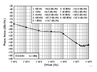
fOSC = 100 MHz Jitter = 55.8 fs (100 Hz - 100 MHz)
fPD = 200 MHz
Figure 3. Closed-Loop Phase Noise at 15 GHz
LMX2595 D004_SNAS696.gif
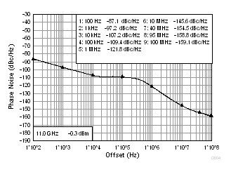
fOSC = 100 MHz Jitter = 46.8 fs (100 Hz - 100 MHz)
fPD = 200 MHz
Figure 5. Closed-Loop Phase Noise at 11 GHz
LMX2595 D001_SNAS696.gif
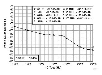
fOSC = 100 MHz Jitter = 46.87 fs (100 Hz - 100 MHz)
fPD = 200 MHz
Figure 7. Closed-Loop Phase Noise at 8 GHz
LMX2595 D012_SNAS696.gif
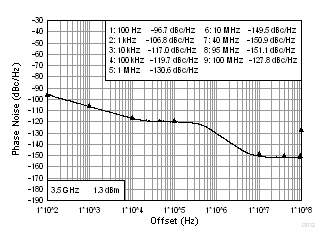
fOSC = 100 MHz fOUT = 14 GHz / 4 = 3.5 GHz
fPD = 200 MHz Jitter = 49.4 fs (100 Hz - 100 MHz)
fVCO = 14 GHz
Figure 9. Closed-Loop Phase Noise at 3.5 GHz
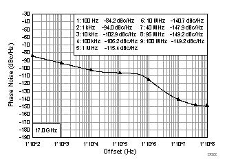
LMX2595 D022_SNAS696.gif
fOSC = 100 MHz fOUT = 2 × 8.5 GHz = 17 GHz
fPD = 200 MHz Jitter = 55.0 fs (100 Hz - 100 MHz)
Figure 11. Closed-Loop Phase Noise at 17 GHz
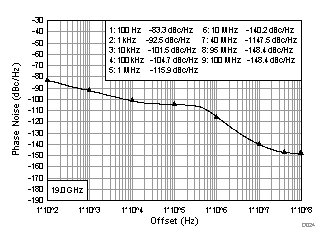
LMX2595 D024_SNAS696.gif
fOSC = 100 MHz fOUT = 2 × 9.5 GHz = 19 GHz
fPD = 200 MHz Jitter = 54.7 fs (100 Hz - 100 MHz)
Figure 13. Closed-Loop Phase Noise at 19 GHz
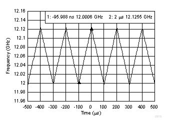
LMX2595 D010_SNAS696.gif
Figure 15. VCO Ramping 12-GHz to 12.125-GHz Calibration Free
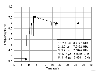
LMX2595 D008_SNAS696.gif
CalTime = 33.6 µs = 5.8 µs (Core) + 14 µs (Fcal) + 13.8 µs (Ampcal)
fOSC = 200 MHz, fPD = 100 MHz, fVCO = 7.5 - 14 GHz, CHDIV = 2
Figure 17. VCO Unassisted Calibration
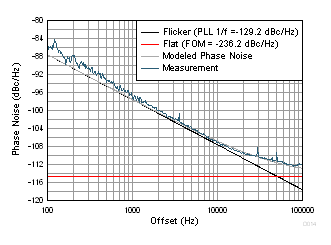
LMX2595 tc_pllnoisemetrics.gif
fVCO = 12 GHz fPD = 100 MHz
Figure 19. Calculation of PLL Noise Metrics
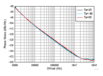
LMX2595 tc_PhaseNoiseVsTemp.gif
fVCO = 8 GHz, Narrow Loop Bandwidth (<100 Hz)
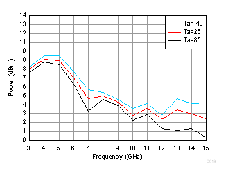
Figure 21. VCO Phase Noise Over Temperature
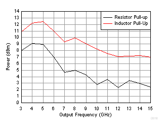
LMX2595 tc_powervspullup.gif
Single-Ended Output OUTx_PWR = 50
VCO2X_EN = 0
Figure 23. Output Power Across Frequency
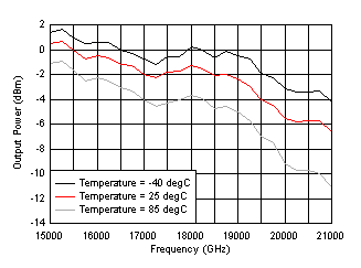
LMX2595 D034_SNAS696.gif
Single-ended output with resistor pullup. OUTA_PWR = 20
DBLR_IBIAS_CTRL1 = 3115
Figure 25. Output Power vs. Temperature With Doubler
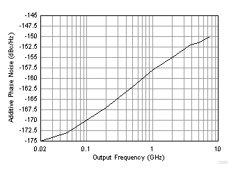
LMX2595 tc_dividernoise.gif
This noise adds to the scaled VCO Noise when the channel divider is used.
Figure 27. Additive VCO Divider Noise Floor
LMX2595 D003_SNAS696.gif
fOSC = 100 MHz Jitter = 52.6 fs (100 Hz - 100 MHz)
fPD = 200 MHz
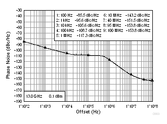
Figure 4. Closed-Loop Phase Noise at 13 GHz
LMX2595 D005_SNAS696.gif
fOSC = 100 MHz Jitter = 46.9 fs (100 Hz - 100 MHz)
fPD = 200 MHz
Figure 6. Closed-Loop Phase Noise at 9 GHz
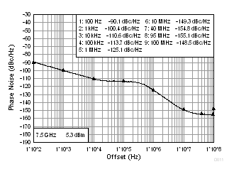
LMX2595 D011_SNAS696.gif
fOSC = 100 MHz Jitter = 44.1 fs (100 Hz - 100 MHz)
fPD = 200 MHz
Figure 8. Closed-Loop Phase Noise at 7.5 GHz
LMX2595 D016_SNAS696.gif
fOSC = 100 MHz fOUT = 2 × 8 GHz = 16 GHz
fPD = 200 MHz Jitter = 52.9 fs (100 Hz - 100 MHz)
Figure 10. Closed-Loop Phase Noise at 16 GHz
LMX2595 D023_SNAS696.gif
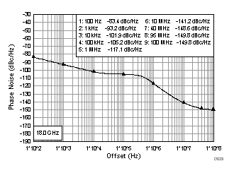
fOSC = 100 MHz fOUT = 2 × 9 GHz = 18 GHz
fPD = 200 MHz Jitter = 52.6 fs (100 Hz - 100 MHz)
Figure 12. Closed-Loop Phase Noise at 18 GHz
LMX2595 D025_SNAS696.gif
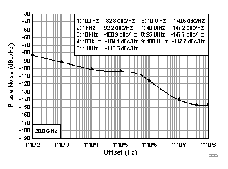
fOSC = 100 MHz fOUT = 2 × 10 GHz = 20 GHz
fPD = 200 MHz Jitter = 52.7 fs (100 Hz - 100 MHz)
Figure 14. Closed-Loop Phase Noise at 20 GHz
LMX2595 D013_SNAS696.gif
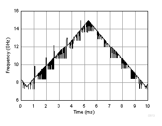
The glitches in the plot are due to the inability of the measurement equipment to track the VCO while calibrating.
Figure 16. VCO Ramping 7.5-GHz to 15-GHz Triangle Wave With VCO Calibration
LMX2595 D009_SNAS696.gif
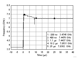
CalTime = 25.2 µs = 1.3 µs (Core) + 9.1 µs (Fcal) +14.8 µs (Ampcal)
fOSC = 200 MHz, fPD = 100 MHz, fVCO = 7.5 GHz - 14 GHz, CHDIV = 2
Figure 18. VCO Calibration With Partial Assist
LMX2595 tc_fpdimpact.gif
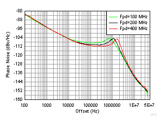
fOSC = 200 MHz fVCO = 14.8 GHz
Figure 20. PLL Phase Noise Variation vs. fPD
LMX2595 tc_PhaseNoiseVsTempDelta.gif
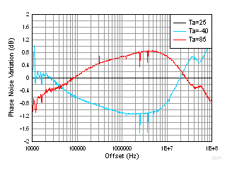
fVCO = 8 GHz, Narrow Loop Bandwidth (<100 Hz)
Figure 22. CHANGE in 8-GHz VCO Phase Noise Over Temperature
LMX2595 tc_powervstemp.gif
Single-ended output with resistor pullup and OUTx_PWR = 50. Note that Near 13.3 to 14.3 GHz, output power can be impacted at hot temperature. See the Application Information section for more information.
Figure 24. Output Power vs Temperature Without Doubler
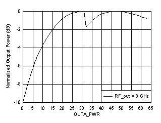
LMX2595 D030_SNAS696.gif
Resistor pullup Normalized to maximum output power.
Figure 26. Output Power Normalized To Maximum Across OUTA_PWR With Resistor Pullup