ZHCSEI5A March 2013 – January 2016 LMX2485Q-Q1
PRODUCTION DATA.
- 1 特性
- 2 应用范围
- 3 说明
- 4 修订历史记录
- 5 Pin Configuration and Functions
- 6 Specifications
- 7 Parameter Measurement Information
-
8 Detailed Description
- 8.1 Overview
- 8.2 Functional Block Diagram
- 8.3 Feature Description
- 8.4 Device Functional Modes
- 8.5 Programming
- 8.6 Register Maps
- 9 Application and Implementation
- 10Power Supply Recommendations
- 11Layout
- 12器件和文档支持
- 13机械、封装和可订购信息
封装选项
请参考 PDF 数据表获取器件具体的封装图。
机械数据 (封装 | 引脚)
- RTW|24
散热焊盘机械数据 (封装 | 引脚)
- RTW|24
订购信息
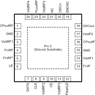
5 Pin Configuration and Functions
RTW Package
24-Pin WQFN
Top View

Pin Functions
| PIN | I/O | DESCRIPTION | |
|---|---|---|---|
| NAME | NO. | ||
| CE | 10 | I | Chip Enable control pin. Must be pulled high for normal operation. |
| CLK | 8 | I | MICROWIRE Clock. High-impedance CMOS Clock input. Data for the various counters is clocked into the 24 bit shift register on the rising edge |
| CPoutIF | 16 | O | IF PLL charge pump output |
| CPoutRF | 1 | O | RF PLL charge pump output. |
| DATA | 7 | I | MICROWIRE Data. High-impedance binary serial data input. |
| ENOSC | 19 | I | Oscillator enable. When this is set to high, the OSCout pin is enabled regardless of the state of other pins or register bits. |
| FinIF | 13 | I | IF PLL high-frequency input pin. |
| FinRF | 4 | I | RF PLL high-frequency input pin. |
| FinRF* | 5 | I | RF PLL complementary high-frequency input pin. Shunt to ground with a 100-pF capacitor. |
| FLoutRF | 23 | O | RF PLL Fastlock Output. Also functions as Programmable TRI-STATE CMOS output. |
| Ftest/LD | 12 | O | Test frequency output / Lock Detect. |
| GND | 0 | — | Ground Substrate. This is on the bottom of the package and must be grounded. |
| GND | 2 | — | RF PLL analog ground. |
| GND | 15 | — | IF PLL digital ground. |
| LE | 6 | I | MICROWIRE Load Enable. High impedance CMOS input. Data stored in the shift registers is loaded into the internal latches when LE goes HIGH |
| NC | 21 | I | This pin must be left open. |
| OSCin | 20 | I | Input for TCXO signal. |
| OSCout | 18 | O | Buffered output of the OSCin signal. |
| VddRF1 | 3 | — | RF PLL analog power supply. |
| VddRF2 | 9 | — | Power supply for RF PLL digital circuitry. |
| VddRF3 | 22 | — | Power supply for RF PLL digital circuitry. |
| VddRF4 | 24 | — | RF PLL analog power supply. |
| VddIF1 | 14 | — | IF PLL analog power supply. |
| VddIF2 | 17 | — | IF PLL power supply. |