ZHCSGZ1 October   2017 LMT84-Q1

PRODUCTION DATA.  

  1. 特性
  2. 应用
  3. 说明
  4. 修订历史记录
  5. Device Comparison Tables
  6. Pin Configuration and Functions
  7. Specifications
    1. 7.1 Absolute Maximum Ratings
    2. 7.2 ESD Ratings
    3. 7.3 Recommended Operating Conditions
    4. 7.4 Thermal Information
    5. 7.5 Accuracy Characteristics
    6. 7.6 Electrical Characteristics
    7. 7.7 Typical Characteristics
  8. Detailed Description
    1. 8.1 Overview
    2. 8.2 Functional Block Diagram
    3. 8.3 Feature Description
      1. 8.3.1 LMT84 Transfer Function
    4. 8.4 Device Functional Modes
      1. 8.4.1 Mounting and Thermal Conductivity
      2. 8.4.2 Output Noise Considerations
      3. 8.4.3 Capacitive Loads
      4. 8.4.4 Output Voltage Shift
  9. Application and Implementation
    1. 9.1 Applications Information
    2. 9.2 Typical Applications
      1. 9.2.1 Connection to an ADC
        1. 9.2.1.1 Design Requirements
        2. 9.2.1.2 Detailed Design Procedure
        3. 9.2.1.3 Application Curve
      2. 9.2.2 Conserving Power Dissipation With Shutdown
        1. 9.2.2.1 Design Requirements
        2. 9.2.2.2 Detailed Design Procedure
        3. 9.2.2.3 Application Curves
  10. 10Power Supply Recommendations
  11. 11Layout
    1. 11.1 Layout Guidelines
    2. 11.2 Layout Examples
  12. 12器件和文档支持
    1. 12.1 接收文档更新通知
    2. 12.2 社区资源
    3. 12.3 商标
    4. 12.4 静电放电警告
    5. 12.5 Glossary
  13. 13机械、封装和可订购信息

封装选项

机械数据 (封装 | 引脚)
散热焊盘机械数据 (封装 | 引脚)
订购信息

Layout

Layout Guidelines

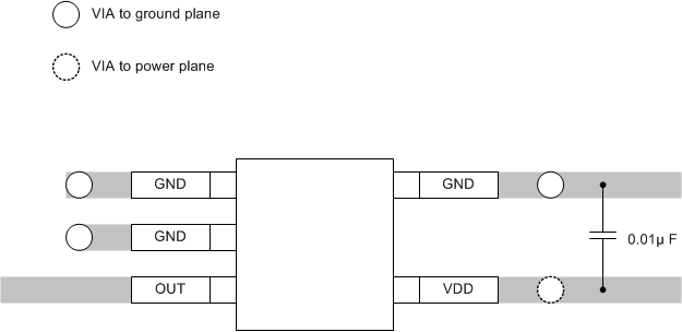
The LMT84-Q1 is extremely simple to layout. If a power-supply bypass capacitor is used, is should be connected as shown in the Layout Examples.

Layout Examples

LMT84-Q1 Layout_SNIS167.gif Figure 19. SC70 Package Recommended Layout