ZHCSP51B december   2020  – may 2023 LMR43610 , LMR43620

PRODUCTION DATA  

  1.   1
  2. 特性
  3. 应用
  4. 说明
  5. Revision History
  6. Device Comparison Table
  7. Pin Configuration and Functions
  8. Specifications
    1. 7.1 Absolute Maximum Ratings
    2. 7.2 ESD Ratings
    3. 7.3 Recommended Operating Conditions
    4. 7.4 Thermal Information
    5. 7.5 Electrical Characteristics
    6. 7.6 System Characteristics
    7. 7.7 Typical Characteristics
  9. Detailed Description
    1. 8.1 Overview
    2. 8.2 Functional Block Diagram
    3. 8.3 Feature Description
      1. 8.3.1  Enable, Start-Up, and Shutdown
      2. 8.3.2  External CLK SYNC (with MODE/SYNC)
        1. 8.3.2.1 Pulse-Dependent MODE/SYNC Pin Control
      3. 8.3.3  Adjustable Switching Frequency (with RT)
      4. 8.3.4  Power-Good Output Operation
      5. 8.3.5  Internal LDO, VCC, and VOUT/FB Input
      6. 8.3.6  Bootstrap Voltage and VBOOT-UVLO (BOOT Terminal)
      7. 8.3.7  Output Voltage Selection
      8. 8.3.8  Soft Start and Recovery from Dropout
        1. 8.3.8.1 Recovery from Dropout
      9. 8.3.9  Current Limit and Short Circuit
      10. 8.3.10 Thermal Shutdown
      11. 8.3.11 Input Supply Current
    4. 8.4 Device Functional Modes
      1. 8.4.1 Shutdown Mode
      2. 8.4.2 Standby Mode
      3. 8.4.3 Active Mode
        1. 8.4.3.1 CCM Mode
        2. 8.4.3.2 Auto Mode – Light-Load Operation
          1. 8.4.3.2.1 Diode Emulation
          2. 8.4.3.2.2 Frequency Reduction
        3. 8.4.3.3 FPWM Mode – Light-Load Operation
        4. 8.4.3.4 Minimum On-Time (High Input Voltage) Operation
        5. 8.4.3.5 Dropout
  10. Application and Implementation
    1. 9.1 Application Information
    2. 9.2 Typical Application
      1. 9.2.1 Design Requirements
      2. 9.2.2 Detailed Design Procedure
        1. 9.2.2.1 Choosing the Switching Frequency
        2. 9.2.2.2 Setting the Output Voltage
          1. 9.2.2.2.1 FB for Adjustable Output
        3. 9.2.2.3 Inductor Selection
        4. 9.2.2.4 Output Capacitor Selection
        5. 9.2.2.5 Input Capacitor Selection
        6. 9.2.2.6 CBOOT
        7. 9.2.2.7 VCC
        8. 9.2.2.8 CFF Selection
          1. 9.2.2.8.1 External UVLO
        9. 9.2.2.9 Maximum Ambient Temperature
      3. 9.2.3 Application Curves
    3. 9.3 Best Design Practices
    4. 9.4 Power Supply Recommendations
    5. 9.5 Layout
      1. 9.5.1 Layout Guidelines
        1. 9.5.1.1 Ground and Thermal Considerations
      2. 9.5.2 Layout Example
  11. 10Device and Documentation Support
    1. 10.1 Device Support
      1. 10.1.1 第三方产品免责声明
      2. 10.1.2 Device Nomenclature
    2. 10.2 Documentation Support
      1. 10.2.1 Related Documentation
    3. 10.3 支持资源
    4. 10.4 Trademarks
    5. 10.5 静电放电警告
    6. 10.6 术语表
  12. 11Mechanical, Packaging, and Orderable Information

封装选项

机械数据 (封装 | 引脚)
散热焊盘机械数据 (封装 | 引脚)
订购信息
Frequency Reduction

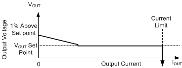
The LMR436x0 reduces frequency whenever output voltage is high. This function is enabled whenever the internal error amplifier compensation output, COMP, an internal signal, is low and there is an offset between the regulation set point of VOUT/FB and the voltage applied to VOUT/FB. The net effect is that there is larger output impedance while lightly loaded in auto mode than in normal operation. Output voltage must be approximately 1% high when the part is completely unloaded.
GUID-DB5E5F0F-79FF-4D0D-AD69-2347C45EB319-low.gif
In auto mode, after output current drops below approximately 1/10th the rated current of the part, output resistance increases so that output voltage is 1% high while the buck is completely unloaded.
Figure 8-17 Steady State Output Voltage Versus Output Current in Auto Mode

In PFM operation, a small DC positive offset is required on the output voltage to activate the PFM detector. The lower the frequency in PFM, the more DC offset is needed on VOUT. If the DC offset on VOUT is not acceptable, a dummy load at VOUT or FPWM mode can be used to reduce or eliminate this offset.