ZHCSJO3B May 2019 – November 2020 LMR34215-Q1
PRODUCTION DATA
- 1 特性
- 2 应用
- 3 说明
- 4 Revision History
- 5 Device Comparison Table
- 6 Pin Configuration and Functions
- 7 Specifications
- 8 Detailed Description
- 9 Power Supply Recommendations
- 10Layout
- 11Device and Documentation Support
- 12Mechanical, Packaging, and Orderable Information
9.2.2.10 Maximum Ambient Temperature
As with any power conversion device, the LMR34215-Q1 dissipates internal power while operating. The effect of this power dissipation is to raise the internal temperature of the converter above ambient. The internal die temperature (TJ) is a function of the ambient temperature, the power loss and the effective thermal resistance, RθJA of the device and PCB combination. The maximum internal die temperature for the LMR34215-Q1 must be limited to 150°C. This establishes a limit on the maximum device power dissipation and therefore the load current. Equation 11 shows the relationships between the important parameters. It is easy to see that larger ambient temperatures (TA) and larger values of RθJA reduce the maximum available output current. The converter efficiency can be estimated by using the curves provided in this data sheet. If the desired operating conditions cannot be found in one of the curves, then interpolation can be used to estimate the efficiency. Alternatively, the EVM can be adjusted to match the desired application requirements and the efficiency can be measured directly. The correct value of RθJA is more difficult to estimate. As stated in Semiconductor and IC Package Thermal Metrics, the values given in are not valid for design purposes and must not be used to estimate the thermal performance of the application. The values reported in that table were measured under a specific set of conditions that are rarely obtained in an actual application.
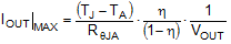
where
- η = efficiency
The effective RθJA is a critical parameter and depends on many factors such as power dissipation, air temperature/flow, PCB area, copper heat-sink area, number of thermal vias under the package, and adjacent component placement to mention just a few. Due to the ultra-miniature size of the VQFN (RNX) package, a DAP is not available. This means that this package exhibits a somewhat greater RθJA. A typical example of RθJA vs copper board area can be found in Figure 9-4. Note that the data given in this graph is for illustration purposes only, and the actual performance in any given application depends on all of the factors mentioned above.
 Package") Figure 9-4 RθJA versus Copper Board Area for the VQFN (RNX) Package
Figure 9-4 RθJA versus Copper Board Area for the VQFN (RNX) PackageUse the following resources as guides to optimal thermal PCB design and estimating RθJA for a given application environment: