ZHCSJO4A May   2019  – October 2019 LMR34206-Q1

PRODUCTION DATA.  

  1. 特性
  2. 应用
  3. 说明
    1.     Device Images
      1. 3.1 简化原理图
  4. 修订历史记录
  5. Device Comparison Table
  6. Pin Configuration and Functions
    1.     Pin Functions
  7. Specifications
    1. 7.1 Absolute Maximum Ratings
    2. 7.2 ESD Ratings
    3. 7.3 Recommended Operating Conditions
    4. 7.4 Thermal Information
    5. 7.5 Electrical Characteristics
    6. 7.6 Timing Requirements
    7. 7.7 System Characteristics
    8. 7.8 Typical Characteristics
  8. Detailed Description
    1. 8.1 Overview
    2. 8.2 Functional Block Diagram
    3. 8.3 Feature Description
      1. 8.3.1 Power-Good Flag Output
      2. 8.3.2 Enable and Start-up
      3. 8.3.3 Current Limit and Short Circuit
      4. 8.3.4 Undervoltage Lockout and Thermal Shutdown
    4. 8.4 Device Functional Modes
      1. 8.4.1 Auto Mode
      2. 8.4.2 Forced PWM Operation
      3. 8.4.3 Dropout
      4. 8.4.4 Minimum Switch On-Time
      5. 8.4.5 Spread Spectrum Operation
  9. Application and Implementation
    1. 9.1 Application Information
    2. 9.2 Typical Application
      1. 9.2.1 Design Requirements
        1. 9.2.1.1 Design Requirements
      2. 9.2.2 Detailed Design Procedure
        1. 9.2.2.1 Choosing the Switching Frequency
        2. 9.2.2.2 Setting the Output Voltage
        3. 9.2.2.3 Inductor Selection
        4. 9.2.2.4 Output Capacitor Selection
        5. 9.2.2.5 Input Capacitor Selection
        6. 9.2.2.6 CBOOT
        7. 9.2.2.7 VCC
        8. 9.2.2.8 External UVLO
        9. 9.2.2.9 Maximum Ambient Temperature
      3. 9.2.3 Application Curves
  10. 10Power Supply Recommendations
  11. 11Layout
    1. 11.1 Layout Guidelines
      1. 11.1.1 Ground and Thermal Considerations
    2. 11.2 Layout Example
  12. 12器件和文档支持
    1. 12.1 器件支持
      1. 12.1.1 开发支持
    2. 12.2 文档支持
      1. 12.2.1 相关文档
    3. 12.3 接收文档更新通知
    4. 12.4 支持资源
    5. 12.5 商标
    6. 12.6 静电放电警告
    7. 12.7 Glossary
  13. 13机械、封装和可订购信息

封装选项

机械数据 (封装 | 引脚)
散热焊盘机械数据 (封装 | 引脚)
订购信息

Application Curves

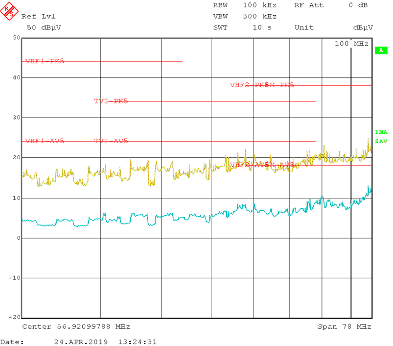
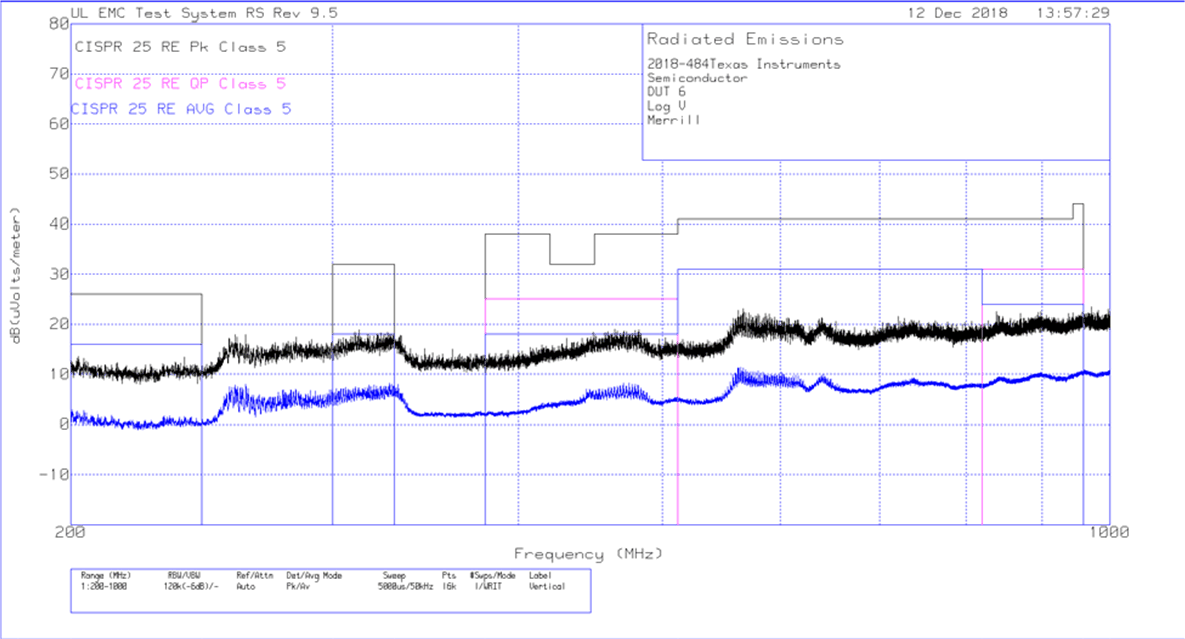
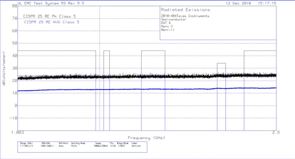
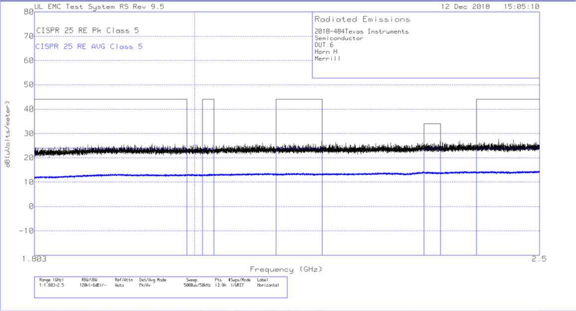
Unless otherwise specified the following conditions apply: VIN = 12 V, TA = 25°C. The circuit is shown in Figure 18, with the BOM from Table 5. through Figure 35 show the conducted and radiated emissions performance tested against the CISPR25 Class 5 limits. For the conducted EMI results the limit lines labeled "AV5" represent the average limits, and the limit lines labeled "PK5" represent the peak limits. For the radiated EMI results the blue limit lines represent the average limits, and the black limit lines represent the peak limits.
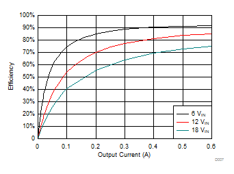
LMR34206-Q1 D007-LMR36006FSC-3p3Vout-Efficiency-snvsay7.gif
VOUT = 3.3 V 2100 kHz
Figure 21. Efficiency
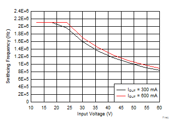
LMR34206-Q1 Frequenc-Foldback-06fsc.gif
VOUT = 3.3 V 2100 kHz
Figure 23. Switching Frequency vs Input Voltage
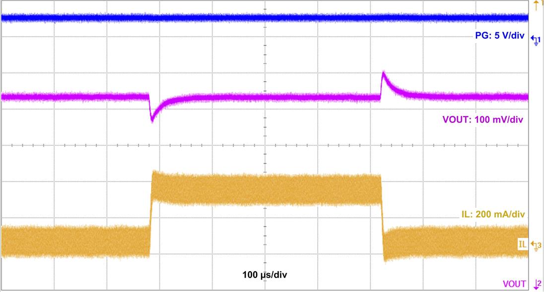
LMR34206-Q1 waveform-08-LMR36006FSC-3P3VOUT-LT-12VIN-300MA-snvsay7.jpg
VOUT = 3.3 V 2100 kHz ILOAD= 10 mA - 0.3 A
Slew Rate = 1 A/µs
Figure 25. Load Transient
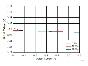
LMR34206-Q1 D009-LMR36006FSC-3P3Vout-loadreg-snvsay7.gif
VOUT = 3.3 V 2100 kHz
Figure 22. Load Regulation
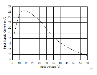
LMR34206-Q1 iqvin_LMR360-6fsc_rtm.gif
VOUT = 3.3 V 2100 kHz
Figure 24. Input Supply Current
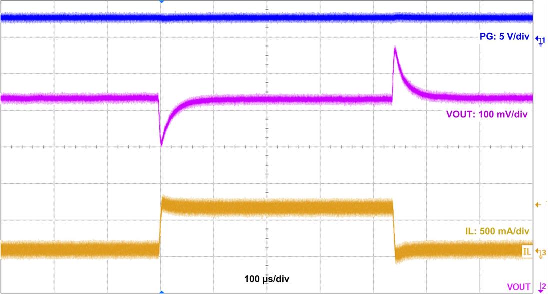
LMR34206-Q1 waveform-09-LMR36006FSC-3p3vout-lt-12vin-600ma-snvsay7.jpg
VOUT = 3.3 V 2100 kHz ILOAD= 10 mA - 0.6 A
Slew Rate = 1 A/µs
Figure 26. Load Transient
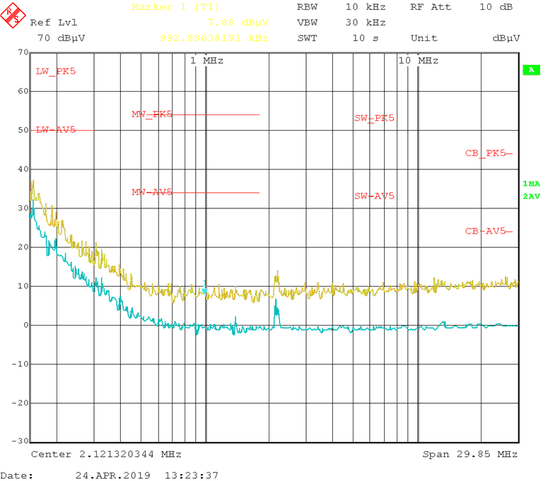
LMR34206-Q1 conducted_low.gif
VIN = 13.5 V VOUT = 5 V IOUT = 1.5 A
Frequency Tested: 150kHz to 30 MHz
Figure 27. Conducted EMI vs. CISPR25 Limits (Yellow: Peak Signal, Blue: Average Signal)
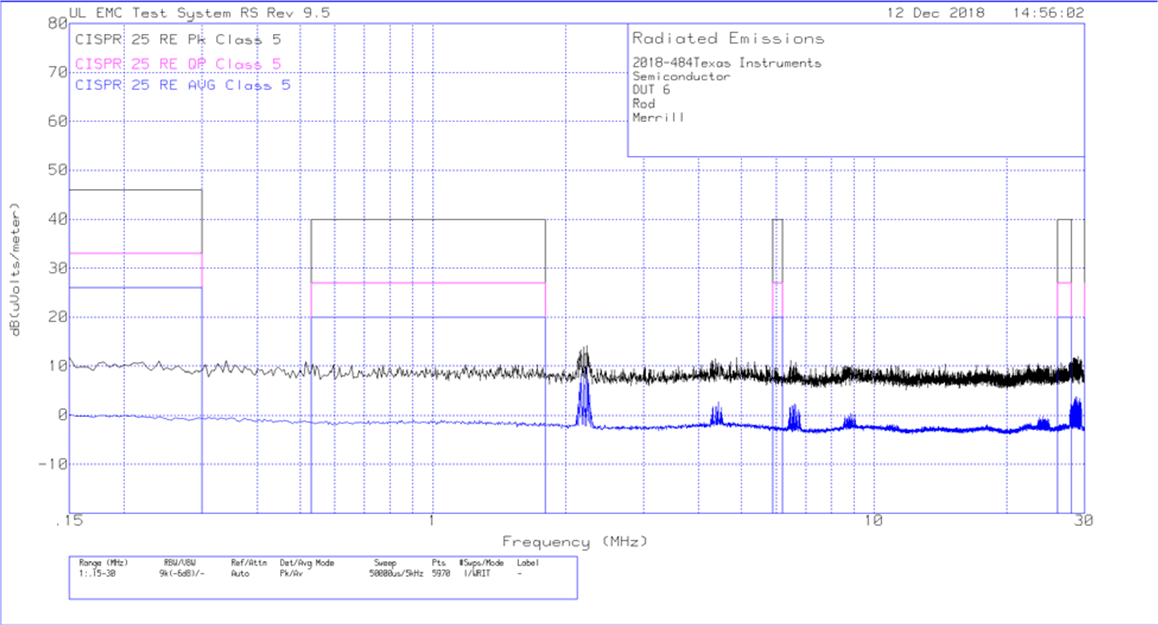
LMR34206-Q1 rod.gif
VIN = 13.5 V VOUT = 5 V IOUT = 1.5 A
Frequency Tested: 150 kHz to 30 MHz
Figure 29. Radiated EMI Rod vs. CISPR25 Limits
LMR34206-Q1 bicon_horizontal.gif
VIN = 13.5 V VOUT = 5 V IOUT = 1.5 A
Frequency Tested: 30 MHz to 200 MHz
Figure 31. Radiated EMI Bicon Horizontal vs. CISPR25 Limits
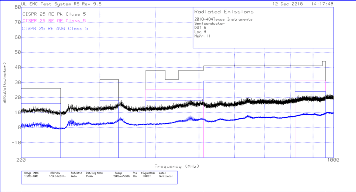
LMR34206-Q1 log_horizaontal.gif
VIN = 13.5 V VOUT = 5 V IOUT = 1.5 A
Frequency Tested: 200 MHz to 1 GHz
Figure 33. Radiated EMI Log Horizontal vs. CISPR25 Limits
LMR34206-Q1 horn_horizontal.gif
VIN = 13.5 V VOUT = 5 V IOUT = 1.5 A
Frequency Tested: 1.8 GHz to 2.5 GHz
Figure 35. Radiated EMI Horn Horizontal vs. CISPR25 Limits
LMR34206-Q1 conducted_high.gif
VIN = 13.5 V VOUT = 5 V IOUT = 1.5 A
Frequency Tested: 30 MHz to 108 MHz
Figure 28. Conducted EMI vs. CISPR25 Limits (Yellow: Peak Signal, Blue: Average Signal)
LMR34206-Q1 bicon_vert.gif
VIN = 13.5 V VOUT = 5 V IOUT = 1.5 A
Frequency Tested: 30 MHz to 200 MHz
Figure 30. Radiated EMI Bicon Vertical vs. CISPR25 Limits
LMR34206-Q1 log_vertical.gif
VIN = 13.5 V VOUT = 5 V IOUT = 1.5 A
Frequency Tested: 200 MHz to 1 GHz
Figure 32. Radiated EMI Log Vertical vs. CISPR25 Limits
LMR34206-Q1 horn_vertical.gif
VIN = 13.5 V VOUT = 5 V IOUT = 1.5 A
Frequency Tested: 1.83 GHz to 2.5 GHz
Figure 34. Radiated EMI Horn Vertical vs. CISPR25 Limits
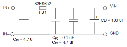
LMR34206-Q1 lmr342xx-emi-schematic-snvsba9.gif
Figure 36. Recommended Input EMI Filter