ZHCSJO4A May   2019  – October 2019 LMR34206-Q1

PRODUCTION DATA.  

  1. 特性
  2. 应用
  3. 说明
    1.     Device Images
      1. 3.1 简化原理图
  4. 修订历史记录
  5. Device Comparison Table
  6. Pin Configuration and Functions
    1.     Pin Functions
  7. Specifications
    1. 7.1 Absolute Maximum Ratings
    2. 7.2 ESD Ratings
    3. 7.3 Recommended Operating Conditions
    4. 7.4 Thermal Information
    5. 7.5 Electrical Characteristics
    6. 7.6 Timing Requirements
    7. 7.7 System Characteristics
    8. 7.8 Typical Characteristics
  8. Detailed Description
    1. 8.1 Overview
    2. 8.2 Functional Block Diagram
    3. 8.3 Feature Description
      1. 8.3.1 Power-Good Flag Output
      2. 8.3.2 Enable and Start-up
      3. 8.3.3 Current Limit and Short Circuit
      4. 8.3.4 Undervoltage Lockout and Thermal Shutdown
    4. 8.4 Device Functional Modes
      1. 8.4.1 Auto Mode
      2. 8.4.2 Forced PWM Operation
      3. 8.4.3 Dropout
      4. 8.4.4 Minimum Switch On-Time
      5. 8.4.5 Spread Spectrum Operation
  9. Application and Implementation
    1. 9.1 Application Information
    2. 9.2 Typical Application
      1. 9.2.1 Design Requirements
        1. 9.2.1.1 Design Requirements
      2. 9.2.2 Detailed Design Procedure
        1. 9.2.2.1 Choosing the Switching Frequency
        2. 9.2.2.2 Setting the Output Voltage
        3. 9.2.2.3 Inductor Selection
        4. 9.2.2.4 Output Capacitor Selection
        5. 9.2.2.5 Input Capacitor Selection
        6. 9.2.2.6 CBOOT
        7. 9.2.2.7 VCC
        8. 9.2.2.8 External UVLO
        9. 9.2.2.9 Maximum Ambient Temperature
      3. 9.2.3 Application Curves
  10. 10Power Supply Recommendations
  11. 11Layout
    1. 11.1 Layout Guidelines
      1. 11.1.1 Ground and Thermal Considerations
    2. 11.2 Layout Example
  12. 12器件和文档支持
    1. 12.1 器件支持
      1. 12.1.1 开发支持
    2. 12.2 文档支持
      1. 12.2.1 相关文档
    3. 12.3 接收文档更新通知
    4. 12.4 支持资源
    5. 12.5 商标
    6. 12.6 静电放电警告
    7. 12.7 Glossary
  13. 13机械、封装和可订购信息

封装选项

机械数据 (封装 | 引脚)
散热焊盘机械数据 (封装 | 引脚)
订购信息

Typical Application

Figure 18 shows for the LMR34206-Q1. This device is designed to function over a wide range of external components and system parameters. However, the internal compensation is optimized for a certain range of external inductance and output capacitance. As a quick start guide, Table 3 provides typical component values for a range of the most common output voltages.
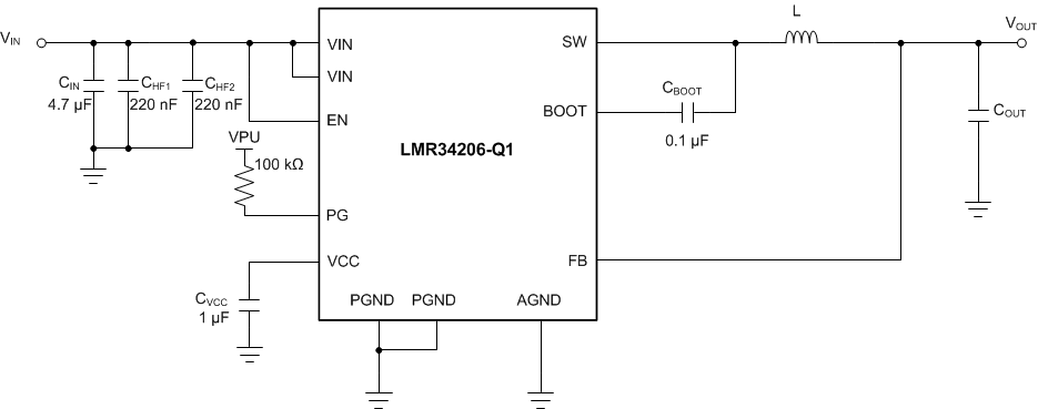
LMR34206-Q1 general_apps_circuit_4206q1-fixed-output.gifFigure 18. Example Applications Circuit (Fixed Output)

Table 3. Typical External Component Values

ƒSW (kHz) VOUT (V) L (µH) Nominal COUT (rated capacitance) (1) Minimum COUT (rated capacitance) (2) CIN
2100 3.3 6.8 2 × 15 µF 1 × 15 µF 4.7 µF + 2 × 220 nF
2100 5 10 2 × 15 µF 1 × 15 µF 4.7 µF + 2 × 220 nF
Optimized for superior load transient performance from 0 to 100% rated load.
Optimized for size constrained end applications.