ZHCSKF5C October 2019 – November 2020 LMR33640
PRODUCTION DATA
- 1 特性
- 2 应用
- 3 说明
- 4 Revision History
- 5 Device Comparison Table
- 6 Pin Configuration and Functions
- 7 Specifications
- 8 Detailed Description
- 9 Application and Implementation
- 10Power Supply Recommendations
- 11Layout
- 12Device and Documentation Support
- 13Mechanical, Packaging, and Orderable Information
6 Pin Configuration and Functions
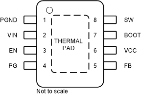
 Figure 6-1 8-Pin HSOIC with PowerPAD™ DDA Package
(Top View)
Figure 6-1 8-Pin HSOIC with PowerPAD™ DDA Package
(Top View)Table 6-1 Pin Functions
| PIN | I/O | DESCRIPTION | |
|---|---|---|---|
| NAME | NO. | ||
| PGND | 1 | G | Power ground terminal. Connect to system ground and AGND. Connect to bypass capacitor with short wide traces. |
| VIN | 2 | P | Input supply to regulator. Connect a high-quality bypass capacitor or capacitors directly to this pin and PGND. |
| EN | 3 | A | Enable input to regulator. High = ON, low = OFF. Can be connected directly to VIN; Do not float. |
| PG | 4 | A | Open drain power-good flag output. Connect to suitable voltage supply through a current limiting resistor. High = power OK, low = power bad. Flag pulls low when EN = Low. Can be left open when not used. |
| FB | 5 | A | Feedback input to regulator. Connect to tap point of feedback voltage divider. Do not float. Do not ground. |
| VCC | 6 | P | Internal 5-V LDO output. Used as supply to internal control circuits. Do not connect to external loads. Can be used as logic supply for power-good flag. Connect a high-quality 1-µF capacitor from this pin to PGND. |
| BOOT | 7 | P | Boot-strap supply voltage for internal high-side driver. Connect a high-quality 100-nF capacitor from this pin to the SW pin. |
| SW | 8 | P | Regulator switch node. Connect to power inductor. |
| AGND | THERMAL PAD |
G | Analog ground for regulator and system. Ground reference for internal references and logic. All electrical parameters are measured with respect to this pin. Connect to system ground on PCB. For the HSOIC package, the pad on the bottom of the device serves as both the AGND connection and a thermal connection to the heat sink ground plane. This pad must be soldered to a ground plane to achieve good electrical and thermal performance. |
| A = Analog, P = Power, G = Ground | |||