ZHCSKF5C October 2019 – November 2020 LMR33640
PRODUCTION DATA
- 1 特性
- 2 应用
- 3 说明
- 4 Revision History
- 5 Device Comparison Table
- 6 Pin Configuration and Functions
- 7 Specifications
- 8 Detailed Description
- 9 Application and Implementation
- 10Power Supply Recommendations
- 11Layout
- 12Device and Documentation Support
- 13Mechanical, Packaging, and Orderable Information
9.2.2.9 External UVLO
In some cases, an input UVLO level different than that provided internal to the device is needed. This can be accomplished by using the circuit shown in Figure 9-2. The input voltage at which the device turns on is designated VON while the turnoff voltage is VOFF. First, a value for RENB is chosen in the range of 10 kΩ to 100 kΩ, then Equation 10 is used to calculate RENT and VOFF.
 Figure 9-2 Setup for External UVLO Application
Equation 10. 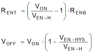
where
- VON = VIN turnon voltage
- VOFF = VIN turnoff voltage