ZHCSHQ4E February 2018 – November 2020 LMR33620
PRODUCTION DATA
- 1 特性
- 2 应用
- 3 说明
- 4 Revision History
- 5 Device Comparison Table
- 6 Pin Configuration and Functions
- 7 Specifications
- 8 Detailed Description
-
9 Application and Implementation
- 9.1 Application Information
- 9.2
Typical Application
- 9.2.1 Design Requirements
- 9.2.2
Detailed Design Procedure
- 9.2.2.1 Custom Design With WEBENCH® Tools
- 9.2.2.2 Choosing the Switching Frequency
- 9.2.2.3 Setting the Output Voltage
- 9.2.2.4 Inductor Selection
- 9.2.2.5 Output Capacitor Selection
- 9.2.2.6 Input Capacitor Selection
- 9.2.2.7 CBOOT
- 9.2.2.8 VCC
- 9.2.2.9 CFF Selection
- 9.2.2.10 External UVLO
- 9.2.2.11 Maximum Ambient Temperature
- 9.2.3 Application Curves
- 9.3 What to Do and What Not to Do
- 10Layout
- 11Device and Documentation Support
封装选项
请参考 PDF 数据表获取器件具体的封装图。
机械数据 (封装 | 引脚)
- RNX|12
- DDA|8
散热焊盘机械数据 (封装 | 引脚)
订购信息
9.2.2.10 External UVLO
In some cases, an input UVLO level different than that provided internal to the device is needed. This can be accomplished by using the circuit shown in Figure 9-2. The input voltage at which the device turns on is designated VON; while the turnoff voltage is VOFF. First, a value for RENB is chosen in the range of 10 kΩ to 100 kΩ and then Equation 10 is used to calculate RENT and VOFF.
 Figure 9-2 Setup for External UVLO Application
Equation 10. 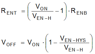
where
- VON = VIN turnon voltage
- VOFF = VIN turnoff voltage