ZHCSCA9A March   2014  – April 2015 LMP92066

PRODUCTION DATA.  

  1. 特性
  2. 应用范围
  3. 说明
  4. 简化电路原理图
  5. 修订历史记录
  6. Pin Configuration and Functions
  7. Specifications
    1. 7.1 Absolute Maximum Ratings
    2. 7.2 ESD Ratings
    3. 7.3 Recommended Operating Conditions
    4. 7.4 Thermal Information
    5. 7.5 Electrical Characteristics
    6. 7.6 Timing Requirements
    7. 7.7 Output Switching Characteristics
    8. 7.8 Typical Characteristics
  8. Detailed Description
    1. 8.1 Overview
    2. 8.2 Functional Block Diagram
    3. 8.3 Features Description
      1. 8.3.1 Temperature Sensor
      2. 8.3.2 Look-Up-Table (LUT) and Arithmetic-Logic Unit (ALU)
        1. 8.3.2.1 LUT and ALU Organization
        2. 8.3.2.2 LUT Coefficient to Register Mapping
        3. 8.3.2.3 The LUT Input and Output Ranges
      3. 8.3.3 Analog Signal Path
        1. 8.3.3.1 DAC
        2. 8.3.3.2 Buffer Amplifier
        3. 8.3.3.3 Output On and Off Control
      4. 8.3.4 Memory
        1. 8.3.4.1 READ and WRITE Access
        2. 8.3.4.2 Access Control
        3. 8.3.4.3 LUT, NOTEPAD Storage, and EEPROM
      5. 8.3.5 I2C Interface
        1. 8.3.5.1 Supported Data Transfer Formats
        2. 8.3.5.2 Slave Address Selection
    4. 8.4 Device Functional Modes
      1. 8.4.1 Default Operating Mode
      2. 8.4.2 Temperature Sensor Override
      3. 8.4.3 ALU Bypass
      4. 8.4.4 DAC Input Override
      5. 8.4.5 LDMOS and GaN Drives
    5. 8.5 Programming
      1. 8.5.1  Temperature Sensor Output Data Access Registers
      2. 8.5.2  DAC Input Data Registers
      3. 8.5.3  Temperature Sensor Status Register
      4. 8.5.4  Override Control Register
      5. 8.5.5  Override Data Registers
      6. 8.5.6  EEPROM Control Register
      7. 8.5.7  Software RESET Register
      8. 8.5.8  Access Control Register
      9. 8.5.9  Block I2C Access Control Register
      10. 8.5.10 I2C Address LOCK Register
      11. 8.5.11 Output Drive Supply Status Register
      12. 8.5.12 Device Version Register
      13. 8.5.13 EEPROM Burn Counter
      14. 8.5.14 LUT Coefficient Registers
      15. 8.5.15 LUT Control Registers
      16. 8.5.16 Notepad Registers
    6. 8.6 Register Map
  9. Application and Implementation
    1. 9.1 Application Information
    2. 9.2 Typical Applications
      1. 9.2.1 Temperature Compensated Bias Generator for LDMOS Power Amplifer (PA)
        1. 9.2.1.1 Design Requirements
        2. 9.2.1.2 Detailed Design Requirements
        3. 9.2.1.3 Application Curves
      2. 9.2.2 Temperature Compensated Bias Generator for GaN Power Amplifer (PA)
        1. 9.2.2.1 Design Requirements
        2. 9.2.2.2 Detailed Design Procedure
        3. 9.2.2.3 Application Curves
    3. 9.3 Do's and Don'ts
      1. 9.3.1 Output Drive Switching
    4. 9.4 Initialization Setup
      1. 9.4.1 Factory Default
      2. 9.4.2 At Power Up
  10. 10Power Supply Recommendations
    1. 10.1 IVDD During EEPROM BURN
    2. 10.2 IVDD During EEPROM TRANSFER
  11. 11Layout
    1. 11.1 Layout Guidelines
    2. 11.2 Layout Example
  12. 12器件和文档支持
    1. 12.1 器件支持
      1. 12.1.1 器件命名规则
    2. 12.2 商标
    3. 12.3 静电放电警告
    4. 12.4 术语表
  13. 13机械、封装和可订购信息

封装选项

机械数据 (封装 | 引脚)
散热焊盘机械数据 (封装 | 引脚)
订购信息

6 Pin Configuration and Functions

PWP Package
16-Pin HTSSOP
Top View
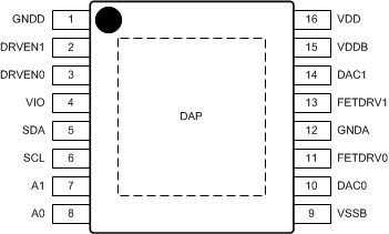
LMP92066 po_TSSOP_snas634.gif

Pin Functions

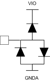
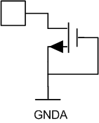
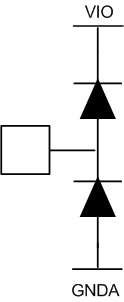
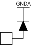
PIN TYPE (1) DESCRIPTION ESD STRUCTURES
NUMBER NAME
1 GNDD G Lower power rail of the digital I/O
LMP92066 pin_one.gif
2:3 DRVEN[1:0] I Asynchronous control of the Changeover Switches
LMP92066 pins_twotosix.gif
4 VIO I Digital I/O power supply rail
5 SDA I/O I2C bi-directional data line
6 SCL I I2C clock input
7:8 A[1:0] I I2C slave address selector
LMP92066 pins_seveight.gif
9 VSSB P Output drive lower supply rail
LMP92066 pin_nine.gif
10, 14 DAC0
DAC1
O DAC0 output
LMP92066 pinsDAC_FETDRV_snas634.gif
11, 13 FETDRV0
FETDRV1
O Gate drive of the external FET device
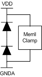
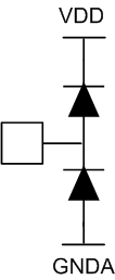
12 GNDA G Analog block lower rail
LMP92066 pin_twelsixteen.gif
15 VDDB P Output drive upper supply rail
LMP92066 pin_fifteen.gif
16 VDD P Analog block upper rail
LMP92066 pin_twelsixteen.gif
--- DAP G Die Attach Pad. For best thermal, and noise performance it should be soldered to the local system ground pad.
LMP92066 DAP.gif
(1) G = Ground; I = Input; O = Output; P = Power