ZHCSCA9A March 2014 – April 2015 LMP92066
PRODUCTION DATA.
- 1 特性
- 2 应用范围
- 3 说明
- 4 简化电路原理图
- 5 修订历史记录
- 6 Pin Configuration and Functions
- 7 Specifications
-
8 Detailed Description
- 8.1 Overview
- 8.2 Functional Block Diagram
- 8.3 Features Description
- 8.4 Device Functional Modes
- 8.5
Programming
- 8.5.1 Temperature Sensor Output Data Access Registers
- 8.5.2 DAC Input Data Registers
- 8.5.3 Temperature Sensor Status Register
- 8.5.4 Override Control Register
- 8.5.5 Override Data Registers
- 8.5.6 EEPROM Control Register
- 8.5.7 Software RESET Register
- 8.5.8 Access Control Register
- 8.5.9 Block I2C Access Control Register
- 8.5.10 I2C Address LOCK Register
- 8.5.11 Output Drive Supply Status Register
- 8.5.12 Device Version Register
- 8.5.13 EEPROM Burn Counter
- 8.5.14 LUT Coefficient Registers
- 8.5.15 LUT Control Registers
- 8.5.16 Notepad Registers
- 8.6 Register Map
- 9 Application and Implementation
- 10Power Supply Recommendations
- 11Layout
- 12器件和文档支持
- 13机械、封装和可订购信息
10 Power Supply Recommendations
The device rails VIO, VDD, and VDDB (VSSB in GaN mode) should be supplied from a well-regulated power supply capable of sourcing at least 50 mA. The required supply levels are shown in the Specifications tables of this document. Along with ceramic bypass capacitors, additional bulk capacitance is recommended on the VDD node. The function of this bulk capacitance is to provide the momentary increases in the supply current requirements due to the EEPROM activity. An electrolytic capacitor with a value of 10 μF to 47 μF is a typical choice.
10.1 IVDD During EEPROM BURN
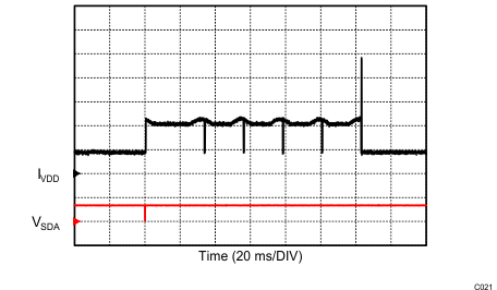
Figure 51 shows the transient behavior of IVDD due to the EEPROM BURN operation. VSDA trace activity is used as the trigger. The triggering event is the BURN command sent via the I2C interface. During the BURN the IVDD increases to almost 4 mA for 125 ms. The 10-mA peaking in IVDD is due to the TRANSFER of newly stored data from EEPROM back to the operating memory – this is part of the internal error detection and correction process.

| IVDD = 2mA/div | VSDA = 5V/div | |
10.2 IVDD During EEPROM TRANSFER
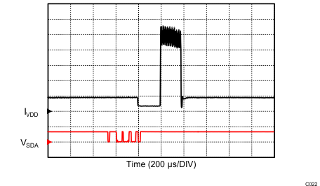
The transfer of data, from the EEPROM to the operating memory, results in the temporary increase in supply current IVDD. The total IVDD increases to about 10 mA for the duration of the TRANFER operation, typically 200 µs. Given the infrequent occurrence, and the short duration, the increased IVDD can be easily supplied by the external bulk capacitors; that is, this does not represent an additional burden to the system power supply. The typical IVDD transient during TRANSFER is shown in Figure 52. The triggering event is the TRANSFER command issued via the I2C interface.

| IVDD = 2mA/div | VSDA = 5V/div | |
The TRANSFER operation occurs due to the following:
- Power-On RESET
- Software RESET
- EEPROM TRANSFER command issued via the I2C interface
- Upon completion of the EEPROM BURN operation, as a data verification step.