ZHCSDM7B February 2012 – December 2014 LMP8646
PRODUCTION DATA.
- 1 特性
- 2 应用
- 3 说明
- 4 修订历史记录
- 5 Pin Configuration and Functions
- 6 Specifications
- 7 Detailed Description
- 8 Application and Implementation
- 9 Power Supply Recommendations
- 10Layout
- 11器件和文档支持
- 12机械、封装和可订购信息
7 Detailed Description
7.1 Overview
The LMP8646 is a single-supply precision current limiter with variable gain selected through an external resistor (RG) and a variable bandwidth selected through an external capacitor (CG) in parallel with RG. Its common-mode of operation is –2 V to 76 V, and the LMP8646 has an buffered output to provide a low-output impedance. More details of the LMP8646's functional description can be seen in the following subsections.
7.2 Functional Block Diagram
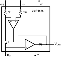
7.3 Feature Description
7.3.1 Theory of Operation
As seen from Figure 26, the sense current flowing through RSENSE develops a voltage drop equal to VSENSE. The high impedance inputs of the amplifier does not conduct this current and the high open-loop gain of the sense amplifier forces its noninverting input to the same voltage as the inverting input. In this way the voltage drop across RIN matches VSENSE. The current IIN flowing through RIN has the following equation:
where
- RIN = 1/Gm = 1/(200 µA/V) = 5 kOhm
IIN flows entirely across the external gain resistor RG to develop a voltage drop equal to:
This voltage is buffered and showed at the output with a very low impedance allowing a very easy interface of the LMP8646 with the feedback of many voltage regulators. This output voltage has the following equation:
where
- Gain = RG/RIN
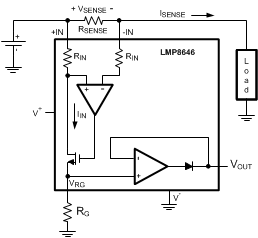 Figure 26. Current Monitor
7.3.1.1 Maximum Output Voltage, VOUT_MAX
The maximum output voltage, VOUT_MAX, depends on the supply voltage, VS = V+ - V-, and on the common-mode voltage, VCM = (+IN + -IN) / 2.
The following subsections show three cases to calculate for VOUT_MAX.
7.3.1.1.1 Case 1: −2 V < VCM < 1.8 V, and VS > 2.7 V
If VS ≥ 5 V,
then VOUT_MAX = 1.3 V.
Else if Vs = 2.7 V,
then VOUT_MAX = 1.1 V.
7.3.1.1.2 Case 2: 1.8 V < VCM < VS, and VS > 3.3 V
In this case, VX is a fixed value that depends on the supply voltage. VX has the following values:
If VS = 12 V, then VX = 10 V.
Else if VS = 5 V, then VX = 3.3 V .
Else if VS = 2.7 V, then VX = 1.1 V.
If VX ≤ (VCM - VSENSE - 0.25) ,
then VOUT_MAX = VX.
Else,
VOUT_MAX = (VCM - VSENSE - 0.25).
For example, if VCM = 4 V, VS = 5 V (and thus VX = 3.3 V), VSENSE = 0.1 V, then VOUT_MAX = 3.3 V because 3.3 V ≤ (4 - 0.1 - 0.25).
7.3.1.1.3 Case 3: VCM > VS, and VS > 2.7 V
If VS = 12 V, then VOUT_MAX = 10 V.
Else if VS = 5 V, then VOUT_MAX = 3.3 V .
Else if VS = 2.7 V, then VOUT_MAX = 1.1 V.
7.4 Device Functional Modes
7.4.1 Output Accuracy
The output accuracy is the device error contributed by the LMP8646 based on its offset and gain errors. The LMP8646 output accuracy has the following equations:
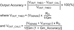
For example, assume VSENSE = 100 mV, RG = 10 kOhm, and it is known that VOFFSET = 1 mV and Gm_Accuracy = 2% (Electrical Characteristics Table), then the output accuracy can be calculated as:

In fact, as VSENSE decreases, the output accuracy worsens as seen in Figure 27. These equations provide a valuable tool to estimate how the LMP8646 affects the overall system performance. Knowing this information allows the system designer to pick the appropriate external resistances (RSENSE and RG) to adjust for the tolerable system error. Examples of this tolerable system error can be seen in the next sections.
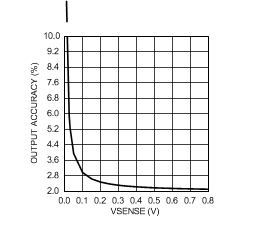 Figure 27. Output Accuracy vs. VSENSE
7.4.2 Selection of the Sense Resistor, RSENSE
The accuracy of the current measurement also depends on the value of the shunt resistor RSENSE. Its value depends on the application and is a compromise between small-signal accuracy and maximum permissible voltage loss in the load line.
RSENSE is directly proportional to VSENSE through the equation RSENSE = (VSENSE) / (ISENSE). If VSENSE is small, then there is a smaller voltage loss in the load line, but the output accuracy is worse because the LMP8646 offset error will contribute more. Therefore, high values of RSENSE provide better output accuracy by minimizing the effects of offset, while low values of RSENSE minimize the voltage loss in the load line. For most applications, best performance is obtained with an RSENSE value that provides a VSENSE of 100 mV to 200 mV.
7.4.2.1 RSENSE Consideration for System Error
The output accuracy described in the previous section talks about the error contributed just by the LMP8646. The system error, however, consists of the errors contributed by the LMP8646 as well as other external resistors such as RSENSE and RG. Let's rewrite the output accuracy equation for the system error assuming that RSENSE is non-ideal and RG is ideal. This equation can be seen as:
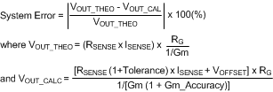
Continuing from the previous output accuracy example, we can calculate for the system error assuming that RSENSE = 100 mOhm (with 1% tolerance), ISENSE = 1A, and RG = 10 kOhm. From the Electrical Characteristics Table, it is also known that VOFFSET = 1 mV and Gm_Accuracy = 2%.
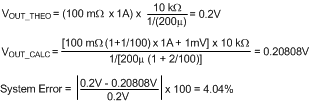
Because an RSENSE tolerance will increase the system error, we recommend selecting an RSENSE resistor with low tolerance.