ZHCSDM7B February   2012  – December 2014 LMP8646

PRODUCTION DATA.  

  1. 特性
  2. 应用
  3. 说明
  4. 修订历史记录
  5. Pin Configuration and Functions
  6. Specifications
    1. 6.1 Absolute Maximum Ratings
    2. 6.2 ESD Ratings
    3. 6.3 Recommended Operating Conditions
    4. 6.4 Thermal Information
    5. 6.5 Electrical Characteristics: 2.7 V
    6. 6.6 Electrical Characteristics: 5 V
    7. 6.7 Electrical Characteristics: 12 V
    8. 6.8 Typical Characteristics
  7. Detailed Description
    1. 7.1 Overview
    2. 7.2 Functional Block Diagram
    3. 7.3 Feature Description
      1. 7.3.1 Theory of Operation
        1. 7.3.1.1 Maximum Output Voltage, VOUT_MAX
          1. 7.3.1.1.1 Case 1: −2 V < VCM < 1.8 V, and VS > 2.7 V
          2. 7.3.1.1.2 Case 2: 1.8 V < VCM < VS, and VS > 3.3 V
          3. 7.3.1.1.3 Case 3: VCM > VS, and VS > 2.7 V
    4. 7.4 Device Functional Modes
      1. 7.4.1 Output Accuracy
      2. 7.4.2 Selection of the Sense Resistor, RSENSE
        1. 7.4.2.1 RSENSE Consideration for System Error
  8. Application and Implementation
    1. 8.1 Application Information
    2. 8.2 Typical Applications
      1. 8.2.1 Application #1: Current Limiter With a Capacitive Load
        1. 8.2.1.1 Design Requirements
        2. 8.2.1.2 Detailed Design Procedure
        3. 8.2.1.3 Application Curve
      2. 8.2.2 Application #2: Current Limiter With a Resistive Load
        1. 8.2.2.1 Design Requirements
        2. 8.2.2.2 Detailed Design Procedure
        3. 8.2.2.3 Application Curve
      3. 8.2.3 Application #3: Current Limiter With a Low-Dropout Regulator and Resistive Load
        1. 8.2.3.1 Design Requirements
        2. 8.2.3.2 Detailed Design Procedure
        3. 8.2.3.3 Application Curve
  9. Power Supply Recommendations
  10. 10Layout
    1. 10.1 Layout Guidelines
    2. 10.2 Layout Example
  11. 11器件和文档支持
    1. 11.1 商标
    2. 11.2 静电放电警告
    3. 11.3 Glossary
  12. 12机械、封装和可订购信息

封装选项

机械数据 (封装 | 引脚)
散热焊盘机械数据 (封装 | 引脚)
订购信息

10 Layout

10.1 Layout Guidelines

  • In a 4-layer board design, the recommended layer stack order from top to bottom is: signal, power, ground, and signal
  • Bypass capacitors should be placed in close proximity to the V+ pin
  • The trace for pins +IN and -IN should be big enough to handle the current running through it.

10.2 Layout Example
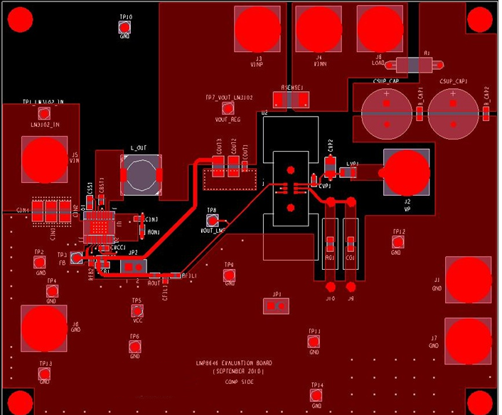
LMP8646 figure 34.pngFigure 34. LMP8646 Evaluation Board Layout