SNOSAT7G August 2007 – October 2015 LMP7300
PRODUCTION DATA.
- 1 Features
- 2 Applications
- 3 Description
- 4 Revision History
- 5 Pin Configuration and Functions
- 6 Specifications
- 7 Detailed Description
- 8 Application and Implementation
- 9 Power Supply Recommendations
- 10Layout
- 11Device and Documentation Support
- 12Mechanical, Packaging, and Orderable Information
10 Layout
10.1 Layout Guidelines
A good PCB layout is always important to reduce output to input coupling. Positive feedback noise reduces performance. For the LMP7300, output coupling is minimized by the unique package pinout. The output is kept away from the noninverting and inverting inputs, the reference and the hysteresis pins.
10.2 Layout Example
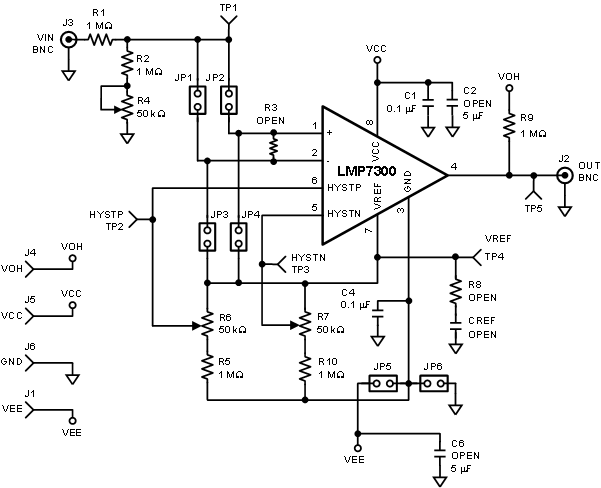
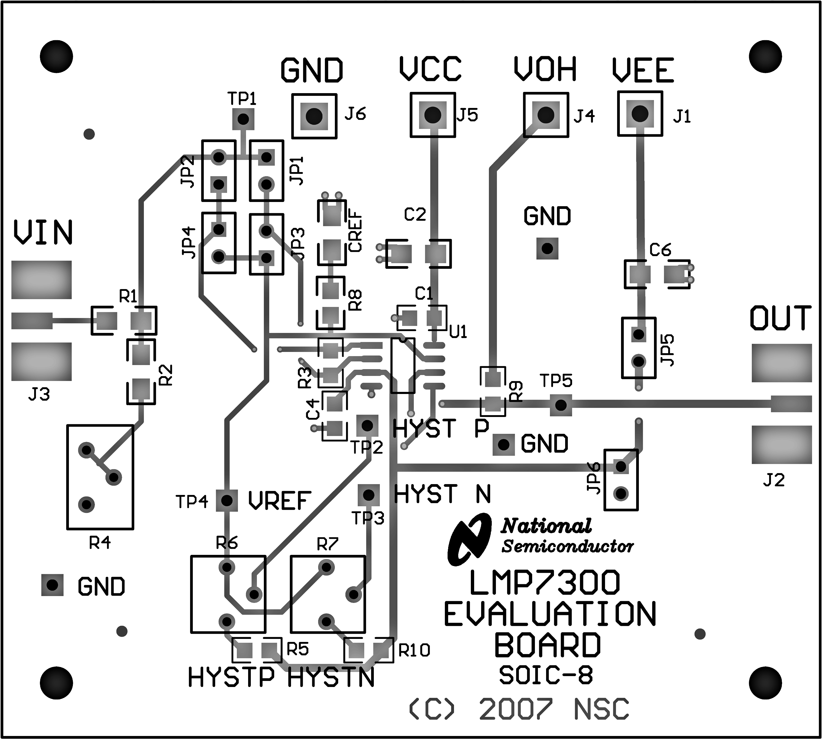
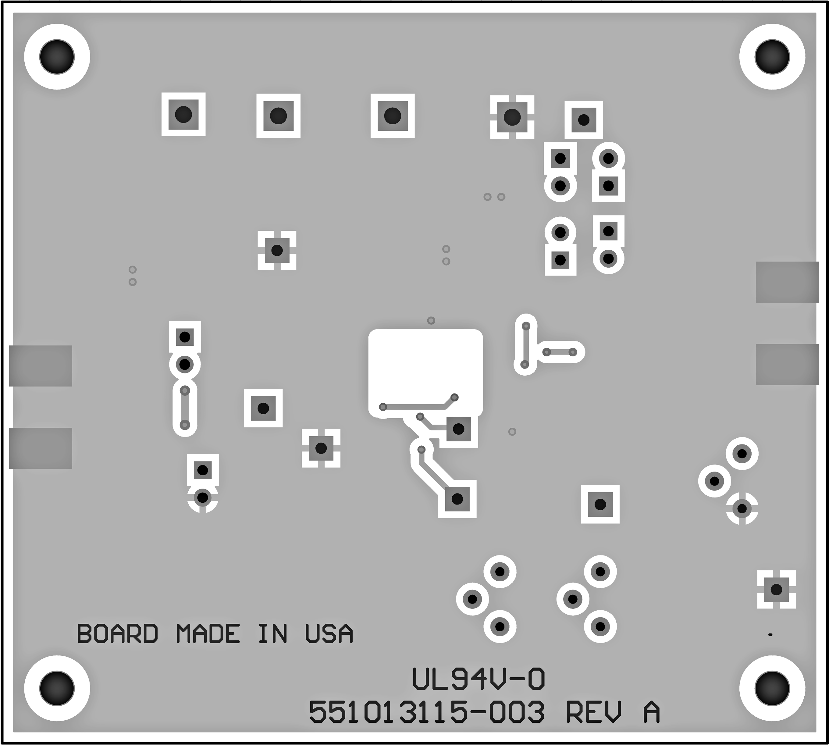
The following section shows an example schematic and layout for the LMP7300MA 8-pin SOIC package.
 Figure 27. LMP7300MA-EVAL Schematic
 Figure 28. LMP7300MA-EVAL Layout Top View
 Figure 29. LMP7300MA-EVAL Layout Bottom View