ZHCSCS5C January 2012 – September 2014 LMH6642Q-Q1 , LMH6643Q-Q1
PRODUCTION DATA.
8 Application and Implementation
NOTE
Information in the following applications sections is not part of the TI component specification, and TI does not warrant its accuracy or completeness. TI’s customers are responsible for determining suitability of components for their purposes. Customers should validate and test their design implementation to confirm system functionality.
8.1 Circuit Description
The LMH664X family is based on Texas Instruments' proprietary VIP10 dielectrically isolated bipolar process.
This device family architecture features the following:
- Complimentary bipolar devices with exceptionally high ft (∼8 GHz) even under low supply voltage (2.7 V) and low bias current.
- A class A-B “turn-around” stage with improved noise, offset, and reduced power dissipation compared to similar speed devices (patent pending).
- Common Emitter push-push output stage capable of 75mA output current (at 0.5V from the supply rails) while consuming only 2.7 mA of total supply current per channel. This architecture allows output to reach within milli-volts of either supply rail.
- Consistent performance over the entire operating supply voltage range with little variation for the most important specifications (for example, BW, SR, IOUT, and so forth).
- Significant power saving (∼40%) compared to competitive devices on the market with similar performance.
8.1.1 Application Hints
This Op Amp family is a drop-in replacement for the AD805X family of high speed Op Amps in most applications. In addition, the LMH664X will typically save about 40% on power dissipation, due to lower supply current, when compared to competition. All AD805X family’s ensured parameters are included in the list of LMH664X ensured specifications in order to ensure equal or better level of performance. However, as in most high performance parts, due to subtleties of applications, it is strongly recommended that the performance of the part to be evaluated is tested under actual operating conditions to ensure full compliance to all specifications.
With 3V supplies and a common mode input voltage range that extends 0.5V below V−, the LMH664X find applications in low voltage/low power applications. Even with 3V supplies, the −3dB BW (@ AV = +1) is typically 115MHz with a tested limit of 80MHz. Production testing ensures that process variations with not compromise speed. High frequency response is exceptionally stable confining the typical −3dB BW over the industrial temperature range to ±2.5%.
As can be seen from the Typical Performance Characteristics, the LMH664X output current capability (∼75mA) is enhanced compared to AD805X. This enhancement, increases the output load range, adding to the LMH664X’s versatility.
Because of the LMH664X’s high output current capability attention should be given to device junction temperature in order not to exceed the Absolute Maximum Rating.
This device family was designed to avoid output phase reversal. With input overdrive, the output is kept near supply rail (or as closed to it as mandated by the closed loop gain setting and the input voltage). See Figure 54:
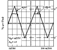 Figure 54. Input and Output Shown with CMVR Exceeded
However, if the input voltage range of −0.5V to 1V from V+ is exceeded by more than a diode drop, the internal ESD protection diodes will start to conduct. The current in the diodes should be kept at or below 10mA.
Output overdrive recovery time is less than 100ns as can be seen from Figure 55 plot:
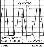 Figure 55. Overload Recovery Waveform
8.1.2 Input and Output Topology
All input / output pins are protected against excessive voltages by ESD diodes connected to V+ and V- rails (see Figure 56). These diodes start conducting when the input / output pin voltage approaches 1Vbe beyond V+ or V- to protect against over voltage. These diodes are normally reverse biased. Further protection of the inputs is provided by the two resistors (R in Figure 56), in conjunction with the string of anti-parallel diodes connected between both bases of the input stage. The combination of these resistors and diodes reduces excessive differential input voltages approaching 2Vbe. The most common situation when this occurs is when the device is used as a comparator (or with little or no feedback) and the device inputs no longer follow each other. In such a case, the diodes may conduct. As a consequence, input current increases and the differential input voltage is clamped. It is important to make sure that the subsequent current flow through the device input pins does not violate the Absolute Maximum Ratings of the device. To limit the current through this protection circuit, extra series resistors can be placed. Together with the built-in series resistors of several hundred ohms, these external resistors can limit the input current to a safe number (i.e. < 10mA). Be aware that these input series resistors may impact the switching speed of the device and could slow down the device.
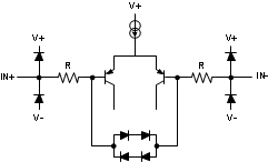 Figure 56. Input Equivalent Circuit
8.2 Single Supply, Low Power Photodiode Amplifier
The circuit shown in Figure 57 is used to amplify the current from a photo-diode into a voltage output. In this circuit, the emphasis is on achieving high bandwidth and the transimpedance gain setting is kept relatively low. Because of its high slew rate limit and high speed, the LMH664X family lends itself well to such an application.
This circuit achieves approximately 1V/mA of transimpedance gain and capable of handling up to 1mApp from the photodiode. Q1, in a common base configuration, isolates the high capacitance of the photodiode (Cd) from the Op Amp input in order to maximize speed. Input is AC coupled through C1 to ease biasing and allow single supply operation. With 5V single supply, the device input/output is shifted to near half supply using a voltage divider from VCC. Note that Q1 collector does not have any voltage swing and the Miller effect is minimized. D1, tied to Q1 base, is for temperature compensation of Q1’s bias point. Q1 collector current was set to be large enough to handle the peak-to-peak photodiode excitation and not too large to shift the U1 output too far from mid-supply.
No matter how low an Rf is selected, there is a need for Cf in order to stabilize the circuit. The reason for this is that the Op Amp input capacitance and Q1 equivalent collector capacitance together (CIN) will cause additional phase shift to the signal fed back to the inverting node. Cf will function as a zero in the feedback path counter-acting the effect of the CIN and acting to stabilized the circuit. By proper selection of Cf such that the Op Amp open loop gain is equal to the inverse of the feedback factor at that frequency, the response is optimized with a theoretical 45° phase margin.
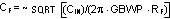
where
Optimized as such, the I-V converter will have a theoretical pole, fp, at:
With Op Amp input capacitance of 3pF and an estimate for Q1 output capacitance of about 3pF as well, CIN = 6pF. From Typical Performance Characteristics, LMH6642/6643 family GBWP is approximately 57 MHz. Therefore, with Rf = 1k, from Equation 1 and Equation 2 above.
Cf = ∼4.1 pF, and fp = 39 MHz
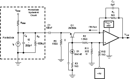 Figure 57. Single Supply Photodiode I-V Converter
For this example, optimum Cf was empirically determined to be around 5pF. This time domain response is shown in Figure 58 below showing about 9 ns rise/fall times, corresponding to about 39 MHz for fp. The overall supply current from the +5 V supply is around 5 mA with no load.
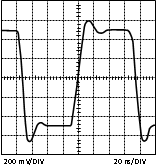 Figure 58. Converter Step Response (1VPP, 20 ns/DIV)
8.3 Printed Circuit Board Layout and Component Values Section
Generally, a good high frequency layout will keep power supply and ground traces away from the inverting input and output pins. Parasitic capacitances on these nodes to ground will cause frequency response peaking and possible circuit oscillations (see Application Note OA-15 (SNOA367) for more information). Texas Instruments suggests the following evaluation boards as a guide for high frequency layout and as an aid in device testing and characterization:
| DEVICE | PACKAGE | EVALUATION BOARD PN |
|---|---|---|
| LMH6642QMF | 5-Pin SOT-23 | LMH730216 |
| LMH6643QMM | 8-Pin VSSOP | LMH730123 |
Another important parameter in working with high speed/high performance amplifiers, is the component values selection. Choosing external resistors that are large in value will effect the closed loop behavior of the stage because of the interaction of these resistors with parasitic capacitances. These capacitors could be inherent to the device or a by-product of the board layout and component placement. Either way, keeping the resistor values lower, will diminish this interaction to a large extent. On the other hand, choosing very low value resistors could load down nodes and will contribute to higher overall power dissipation.