ZHCSCS5C January 2012 – September 2014 LMH6642Q-Q1 , LMH6643Q-Q1
PRODUCTION DATA.
7 Specifications
7.1 Absolute Maximum Ratings(1)(4)(1)
over operating free-air temperature range (unless otherwise noted)| MIN | MAX | UNIT | |
|---|---|---|---|
| VIN Differential | ±2.5 | V | |
| Output Short Circuit Duration | See (2) and (5) | ||
| Supply Voltage (V+ - V−) | 13.5 | V | |
| Voltage at Input/Output pins | V+ +0.8 V− −0.8 |
V | |
| Input Current | ±10 | mA | |
| Junction Temperature (3) | +150 | °C | |
| Soldering Information | |||
| Infrared or Convection Reflow (20 sec) | 235 | °C | |
| Wave Soldering Lead Temp.(10 sec) | 260 | °C | |
(1) Absolute Maximum Ratings indicate limits beyond which damage to the device may occur. Operating Ratings indicate conditions for which the device is intended to be functional, but specific performance is not ensured. For ensured specifications and the test conditions, see the Electrical Characteristics.
(2) Applies to both single-supply and split-supply operation. Continuous short circuit operation at elevated ambient temperature can result in exceeding the maximum allowed junction temperature of 150°C.
(3) The maximum power dissipation is a function of TJ(MAX),R θJA, and TA. The maximum allowable power dissipation at any ambient temperature is PD = (TJ(MAX) - TA)/R θJA. All numbers apply for packages soldered directly onto a PC board.
(4) If Military/Aerospace specified devices are required, please contact the Texas Instruments Sales Office/ Distributors for availability and specifications.
(5) Output short circuit duration is infinite for VS < 6 V at room temperature and below. For VS > 6 V, allowable short circuit duration is 1.5ms.
7.2 Handling Ratings
| MIN | MAX | UNIT | ||||
|---|---|---|---|---|---|---|
| Tstg | Storage temperature range | −65 | +150 | °C | ||
| V(ESD) | Electrostatic discharge | Human body model (HBM), per AEC Q100-002(1) | 2000 | V | ||
| Machine Model (MM)(2) | 200 | |||||
| Charged Device Model (CDM), per AEC Q100-011 | 1000 | |||||
(1) AEC Q100-002 indicates HBM stressing is done in accordance with the ANSI/ESDA/JEDEC JS-001 specification,1.5kΩ in series with 100pF.
(2) Machine Model, 0Ω in series with 200pF.
7.3 Recommended Operating Conditions(1)
over operating free-air temperature range (unless otherwise noted)| MIN | MAX | UNIT | |
|---|---|---|---|
| Supply Voltage (V+ – V−) | 2.7 | 10 | V |
| Operating Temperature Range(2) | −40 | +85 | °C |
(1) Absolute Maximum Ratings indicate limits beyond which damage to the device may occur. Operating Ratings indicate conditions for which the device is intended to be functional, but specific performance is not ensured. For ensured specifications and the test conditions, see the Electrical Characteristics.
(2) The maximum power dissipation is a function of TJ(MAX),RθJA, and TA. The maximum allowable power dissipation at any ambient temperature is PD = (TJ(MAX) - TA)/RθJA. All numbers apply for packages soldered directly onto a PC board.
7.4 Thermal Information
| THERMAL METRIC(1) | DBV05A |
DGK08A |
UNIT | |
|---|---|---|---|---|
| 5 PINS | 8 PINS | |||
| RθJA | Junction-to-ambient thermal resistance(2) | 265°C/W | 235°C/W | °C/W |
(1) For more information about traditional and new thermal metrics, see the IC Package Thermal Metrics application report, SPRA953.
7.5 3V Electrical Characteristics
Unless otherwise specified, all limits ensured for V+ = 3V, V− = 0V, VCM = VO = V+/2, VID (input differential voltage) as noted (where applicable) and RL = 2kΩ to V+/2. Boldface limits apply at the temperature extremes.| PARAMETER | TEST CONDITIONS | MIN(2) | TYP(1) | MAX(2) | UNIT | |
|---|---|---|---|---|---|---|
| BW | −3dB BW | AV = +1, VOUT = 200mVPP | 80 | 115 | MHz | |
| AV = +2, −1, VOUT = 200mVPP | 46 | |||||
| BW0.1dB | 0.1dB Gain Flatness | AV = +2, RL = 150Ω to V+/2, RL = 402Ω, VOUT = 200mVPP |
19 | MHz | ||
| PBW | Full Power Bandwidth | AV = +1, −1dB, VOUT = 1VPP | 40 | MHz | ||
| en | Input-Referred Voltage Noise | f = 100kHz | 17 | nV/√Hz | ||
| f = 1kHz | 48 | |||||
| in | Input-Referred Current Noise | f = 100kHz | 0.90 | pA/√Hz | ||
| f = 1kHz | 3.3 | |||||
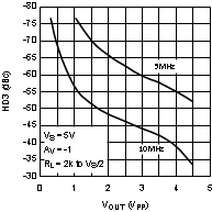
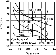
| THD | Total Harmonic Distortion | f = 5MHz, VO = 2VPP, AV = −1, RL = 100Ω to V+/2 |
−48 | dBc | ||
| DG | Differential Gain | VCM = 1V, NTSC, AV = +2 RL =150Ω to V+/2 |
0.17% | |||
| RL =1kΩ to V+/2 | 0.03% | |||||
| DP | Differential Phase | VCM = 1V, NTSC, AV = +2 RL =150Ω to V+/2 |
0.05 | deg | ||
| RL =1kΩ to V+/2 | 0.03 | |||||
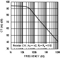
| CT Rej. | Cross-Talk Rejection | f = 5MHz, Receiver: Rf = Rg = 510Ω, AV = +2 |
47 | dB | ||
| TS | Settling Time | VO = 2VPP, ±0.1%, 8pF Load, VS = 5V |
68 | ns | ||
| SR | Slew Rate(6) | AV = −1, VI = 2VPP | 90 | 120 | V/µs | |
| VOS | Input Offset Voltage | For LMH6642 | ±1 | ±5 ±7 |
mV | |
| For LMH6643 | ±1 | ±3.4 ±7 |
||||
| TC VOS | Input Offset Average Drift | (4) | ±5 | µV/°C | ||
| IB | Input Bias Current | (3) | −1.50 | −2.60 −3.25 |
µA | |
| IOS | Input Offset Current | 20 | 800 1000 |
nA | ||
| RIN | Common Mode Input Resistance | 3 | MΩ | |||
| CIN | Common Mode Input Capacitance | 2 | pF | |||
| CMVR | Input Common-Mode Voltage Range | CMRR ≥ 50dB | −0.5 | −0.2 −0.1 |
V | |
| 1.8 1.6 |
2.0 | |||||
| CMRR | Common Mode Rejection Ratio | VCM Stepped from 0V to 1.5V | 72 | 95 | dB | |
| AVOL | Large Signal Voltage Gain | VO = 0.5V to 2.5V RL = 2kΩ to V+/2 |
80 75 |
96 | dB | |
| VO = 0.5V to 2.5V RL = 150Ω to V+/2 |
74 70 |
82 | ||||
| VO | Output Swing High |
RL = 2kΩ to V+/2, VID = 200mV | 2.90 | 2.98 | V | |
| RL = 150Ω to V+/2, VID = 200mV | 2.80 | 2.93 | ||||
| Output Swing Low |
RL = 2kΩ to V+/2, VID = −200mV | 25 | 75 | mV | ||
| RL = 150Ω to V+/2, VID = −200mV | 75 | 150 | ||||
| ISC | Output Short Circuit Current | Sourcing to V+/2 VID = 200mV (5) |
50 35 |
95 | mA | |
| Sinking to V+/2 VID = −200mV (5) |
55 40 |
110 | ||||
| IOUT | Output Current | VOUT = 0.5V from either supply | ±65 | mA | ||
| +PSRR | Positive Power Supply Rejection Ratio | V+ = 3.0V to 3.5V, VCM = 1.5V | 75 | 85 | dB | |
| IS | Supply Current (per channel) | No Load | 2.70 | 4.00 4.50 |
mA | |
(1) Typical values represent the most likely parametric norm.
(2) All limits are ensured by testing or statistical analysis.
(3) Positive current corresponds to current flowing into the device.
(4) Offset voltage average drift determined by dividing the change in VOS at temperature extremes by the total temperature change.
(5) Short circuit test is a momentary test. Output short circuit duration is infinite for VS < 6V at room temperature and below. For VS > 6V, allowable short circuit duration is 1.5ms.
(6) Slew rate is the average of the rising and falling slew rates.
7.6 5V Electrical Characteristics
Unless otherwise specified, all limits ensured for V+ = 5V, V− = 0V, VCM = VO = V+/2, VID (input differential voltage) as noted (where applicable) and RL = 2kΩ to V+/2. Boldface limits apply at the temperature extremes.| PARAMETER | TEST CONDITIONS | MIN(2) | TYP(1) | MAX(2) | UNIT | |
|---|---|---|---|---|---|---|
| BW | −3dB BW | AV = +1, VOUT = 200mVPP | 90 | 120 | MHz | |
| AV = +2, −1, VOUT = 200mVPP | 46 | |||||
| BW0.1dB | 0.1dB Gain Flatness | AV = +2, RL = 150Ω to V+/2, Rf = 402Ω, VOUT = 200mVPP |
15 | MHz | ||
| PBW | Full Power Bandwidth | AV = +1, −1dB, VOUT = 2VPP | 22 | MHz | ||
| en | Input-Referred Voltage Noise | f = 100kHz | 17 | nV/√Hz | ||
| f = 1kHz | 48 | |||||
| in | Input-Referred Current Noise | f = 100kHz | 0.90 | pA/√Hz | ||
| f = 1kHz | 3.3 | |||||
| THD | Total Harmonic Distortion | f = 5MHz, VO = 2VPP, AV = +2 | −60 | dBc | ||
| DG | Differential Gain | NTSC, AV = +2 RL =150Ω to V+/2 |
0.16% | |||
| RL = 1kΩ to V+/2 | 0.05% | |||||
| DP | Differential Phase | NTSC, AV = +2 RL = 150Ω to V+/2 |
0.05 | deg | ||
| RL = 1kΩ to V+/2 | 0.01 | |||||
| CT Rej. | Cross-Talk Rejection | f = 5MHz, Receiver: Rf = Rg = 510Ω, AV = +2 |
47 | dB | ||
| TS | Settling Time | VO = 2VPP, ±0.1%, 8pF Load | 68 | ns | ||
| SR | Slew Rate (3) | AV = −1, VI = 2VPP | 95 | 125 | V/µs | |
| VOS | Input Offset Voltage | For LMH6642 | ±1 | ±5 ±7 |
mV | |
| For LMH6643 | ±1 | ±3.4 ±7 |
||||
| TC VOS | Input Offset Average Drift | (5) | ±5 | µV/°C | ||
| IB | Input Bias Current | (6) | −1.70 | −2.60 −3.25 |
µA | |
| IOS | Input Offset Current | 20 | 800 1000 |
nA | ||
| RIN | Common Mode Input Resistance | 3 | MΩ | |||
| CIN | Common Mode Input Capacitance | 2 | pF | |||
| CMVR | Input Common-Mode Voltage Range | CMRR ≥ 50dB | −0.5 | −0.2 −0.1 |
V | |
| 3.8 3.6 |
4.0 | |||||
| CMRR | Common Mode Rejection Ratio | VCM Stepped from 0V to 3.5V | 72 | 95 | dB | |
| AVOL | Large Signal Voltage Gain | VO = 0.5V to 4.50V RL = 2kΩ to V+/2 |
86 82 |
98 | dB | |
| VO = 0.5V to 4.25V RL = 150Ω to V+/2 |
76 72 |
82 | ||||
| VO | Output Swing High |
RL = 2kΩ to V+/2, VID = 200mV | 4.90 | 4.98 | V | |
| RL = 150Ω to V+/2, VID = 200mV | 4.65 | 4.90 | ||||
| Output Swing Low |
RL = 2kΩ to V+/2, VID = −200mV | 25 | 100 | mV | ||
| RL = 150Ω to V+/2, VID = −200mV | 100 | 150 | ||||
| ISC | Output Short Circuit Current | Sourcing to V+/2 VID = 200mV (4) |
55 40 |
115 | mA | |
| Sinking to V+/2 VID = −200mV (4) |
70 55 |
140 | ||||
| IOUT | Output Current | VO = 0.5V from either supply | ±70 | mA | ||
| +PSRR | Positive Power Supply Rejection Ratio | V+ = 4.0V to 6V | 79 | 90 | dB | |
| IS | Supply Current (per channel) | No Load | 2.70 | 4.25 5.00 |
mA | |
(1) Typical values represent the most likely parametric norm.
(2) All limits are ensured by testing or statistical analysis.
(3) Slew rate is the average of the rising and falling slew rates.
(4) Short circuit test is a momentary test. Output short circuit duration is infinite for VS < 6V at room temperature and below. For VS > 6V, allowable short circuit duration is 1.5ms.
(5) Offset voltage average drift determined by dividing the change in VOS at temperature extremes by the total temperature change.
(6) Positive current corresponds to current flowing into the device.
7.7 ±5V Electrical Characteristics
Unless otherwise specified, all limits ensured for V+ = 5V, V− = −5V, VCM = VO = 0V, VID (input differential voltage) as noted (where applicable) and RL = 2kΩ to ground. Boldface limits apply at the temperature extremes.| PARAMETER | TEST CONDITIONS | MIN(2) | TYP(1) | MAX(2) | UNIT | |
|---|---|---|---|---|---|---|
| BW | −3dB BW | AV = +1, VOUT = 200mVPP | 95 | 130 | MHz | |
| AV = +2, −1, VOUT = 200mVPP | 46 | |||||
| BW0.1dB | 0.1dB Gain Flatness | AV = +2, RL = 150Ω to V+/2, Rf = 806Ω, VOUT = 200mVPP |
12 | MHz | ||
| PBW | Full Power Bandwidth | AV = +1, −1dB, VOUT = 2VPP | 24 | MHz | ||
| en | Input-Referred Voltage Noise | f = 100kHz | 17 | nV/√Hz | ||
| f = 1kHz | 48 | |||||
| in | Input-Referred Current Noise | f = 100kHz | 0.90 | pA/√Hz | ||
| f = 1kHz | 3.3 | |||||
| THD | Total Harmonic Distortion | f = 5MHz, VO = 2VPP, AV = +2 | −62 | dBc | ||
| DG | Differential Gain | NTSC, AV = +2 RL = 150Ω to V+/2 |
0.15% | |||
| RL = 1kΩ to V+/2 | 0.01% | |||||
| DP | Differential Phase | NTSC, AV = +2 RL = 150Ω to V+/2 |
0.04 | deg | ||
| RL = 1kΩ to V+/2 | 0.01 | |||||
| CT Rej. | Cross-Talk Rejection | f = 5MHz, Receiver: Rf = Rg = 510Ω, AV = +2 |
47 | dB | ||
| TS | Settling Time | VO = 2VPP, ±0.1%, 8pF Load, VS = 5V |
68 | ns | ||
| SR | Slew Rate (3) | AV = −1, VI = 2VPP | 100 | 135 | V/µs | |
| VOS | Input Offset Voltage | For LMH6642 | ±1 | ±5 ±7 |
mV | |
| For LMH6643 | ±1 | ±3.4 ±7 |
||||
| TC VOS | Input Offset Average Drift | (5) | ±5 | µV/°C | ||
| IB | Input Bias Current | (6) | −1.60 | −2.60 −3.25 |
µA | |
| IOS | Input Offset Current | 20 | 800 1000 |
nA | ||
| RIN | Common Mode Input Resistance | 3 | MΩ | |||
| CIN | Common Mode Input Capacitance | 2 | pF | |||
| CMVR | Input Common-Mode Voltage Range | CMRR ≥ 50dB | −5.5 | −5.2 −5.1 |
V | |
| 3.8 3.6 |
4.0 | |||||
| CMRR | Common Mode Rejection Ratio | VCM Stepped from −5V to 3.5V | 74 | 95 | dB | |
| AVOL | Large Signal Voltage Gain | VO = −4.5V to 4.5V, RL = 2kΩ |
88 84 |
96 | dB | |
| VO = −4.0V to 4.0V, RL = 150Ω |
78 74 |
82 | ||||
| VO | Output Swing High |
RL = 2kΩ, VID = 200mV | 4.90 | 4.96 | V | |
| RL = 150Ω, VID = 200mV | 4.65 | 4.80 | ||||
| Output Swing Low |
RL = 2kΩ, VID = −200mV | −4.96 | −4.90 | V | ||
| RL = 150Ω, VID = −200mV | −4.80 | −4.65 | ||||
| ISC | Output Short Circuit Current | Sourcing to Ground VID = 200mV (4) |
60 35 |
115 | mA | |
| Sinking to Ground VID = −200mV (4) |
85 65 |
145 | ||||
| IOUT | Output Current | VO = 0.5V from either supply | ±75 | mA | ||
| PSRR | Power Supply Rejection Ratio | (V+, V−) = (4.5V, −4.5V) to (5.5V, −5.5V) | 78 | 90 | dB | |
| IS | Supply Current (per channel) | No Load | 2.70 | 4.50 5.50 |
mA | |
(1) Typical values represent the most likely parametric norm.
(2) All limits are ensured by testing or statistical analysis.
(3) Slew rate is the average of the rising and falling slew rates.
(4) Short circuit test is a momentary test. Output short circuit duration is infinite for VS < 6V at room temperature and below. For VS > 6V, allowable short circuit duration is 1.5ms.
(5) Offset voltage average drift determined by dividing the change in VOS at temperature extremes by the total temperature change.
(6) Positive current corresponds to current flowing into the device.
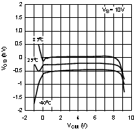
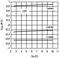
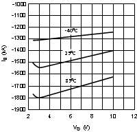
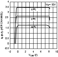
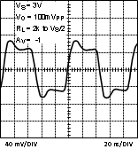
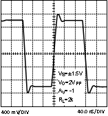
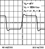
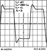
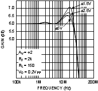
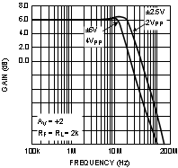
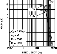
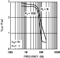
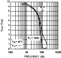
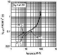
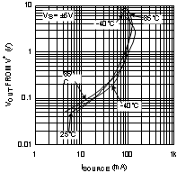
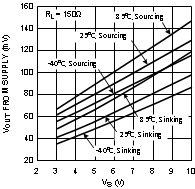
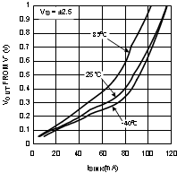
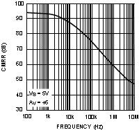
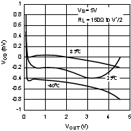
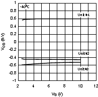
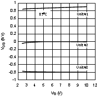
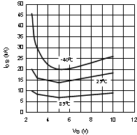
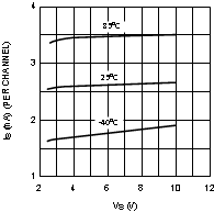
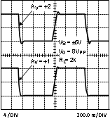
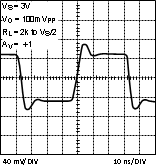
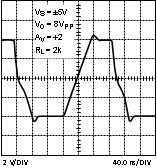
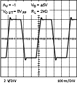
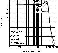
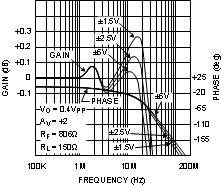
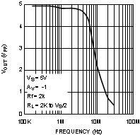
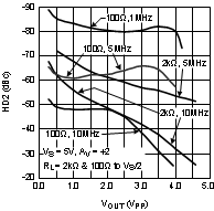
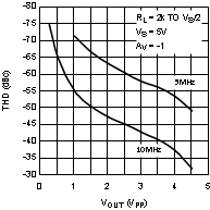
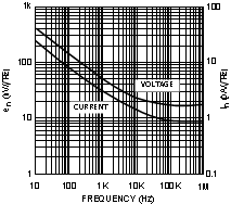
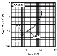
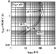
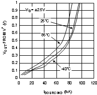
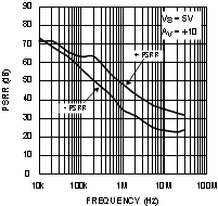
7.8 Typical Performance Characteristics
V+ = +5, V− = −5V, RF = RL = 2kΩ. Unless otherwise specified.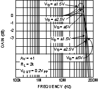
for Various Supplies
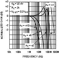
for Various Gain
for Various Supplies
for Various Supplies
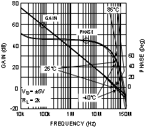
for Various Temperature
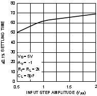
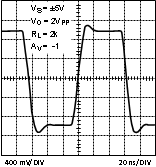
(Output Slew and Settle Time)
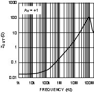
AV = +1
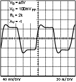
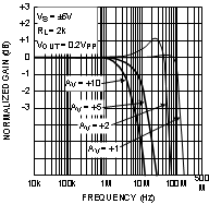
for Various Gain
for Various Temperature
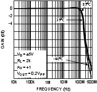
for Various Temperature
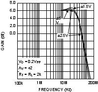
for Various Supplies
for Various Supplies
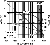
for Various Temperature
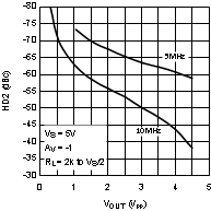
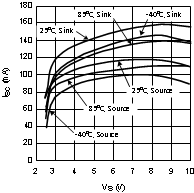
(Output to Output)