ZHCSCR0A August 2014 – December 2014 LMH3401
PRODUCTION DATA.
- 1 特性
- 2 应用
- 3 说明
- 4 修订历史记录
- 5 Device Comparison Table
- 6 Pin Configuration and Functions
- 7 Specifications
- 8 Parameter Measurement Information
- 9 Detailed Description
-
10Application and Implementation
- 10.1 Application Information
- 10.2 Typical Application
- 10.3 Do's and Don'ts
- 11Power-Supply Recommendations
- 12Layout
- 13器件和文档支持
- 14机械封装和可订购信息
13 器件和文档支持
13.1 器件支持
13.1.1 器件命名规则
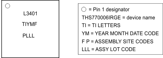 Figure 73. 器件标识信息
13.2 文档支持
13.3 商标
Marki is a trademark of Marki Microwave, Inc.
Rohde & Schwarz is a registered trademark of Rohde & Schwarz.
All other trademarks are the property of their respective owners.
13.4 静电放电警告

ESD 可能会损坏该集成电路。德州仪器 (TI) 建议通过适当的预防措施处理所有集成电路。如果不遵守正确的处理措施和安装程序 , 可能会损坏集成电路。
ESD 的损坏小至导致微小的性能降级 , 大至整个器件故障。 精密的集成电路可能更容易受到损坏 , 这是因为非常细微的参数更改都可能会导致器件与其发布的规格不相符。