ZHCSCR0A August 2014 – December 2014 LMH3401
PRODUCTION DATA.
- 1 特性
- 2 应用
- 3 说明
- 4 修订历史记录
- 5 Device Comparison Table
- 6 Pin Configuration and Functions
- 7 Specifications
- 8 Parameter Measurement Information
- 9 Detailed Description
-
10Application and Implementation
- 10.1 Application Information
- 10.2 Typical Application
- 10.3 Do's and Don'ts
- 11Power-Supply Recommendations
- 12Layout
- 13器件和文档支持
- 14机械封装和可订购信息
9 Detailed Description
9.1 Overview
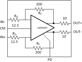
The LMH3401 is a very high-performance, differential amplifier optimized for radio frequency (RF) and intermediate frequency (IF) or high-speed, time-domain applications with signal bandwidths up to 2 GHz. The device is ideal for dc- or ac-coupled applications that may require a single-ended to differential conversion when driving an analog-to-digital converter (ADC). The necessary feedback (RF) and gain set (RG) resistors are fabricated on the device silicon and provide 16 dB of gain when configured for single-ended inputs driven from a 50-Ω source. When used in a fully-differential configuration, 12 dB is obtained when matching the input to a
100-Ω differential. The on-chip resistors simplify PCB implementation and ensure the highest performance over the useable bandwidth of 2 GHz.
A common-mode reference input pin is provided to align the amplifier output common-mode with the ADC input requirements. Power supplies between 3.3 V and 5.0 V can be selected and dual-supply operation is supported when required by the application. A power-down feature is also available for power savings.
In addition to the on-chip feedback resistors, the LMH3401 offers two on-chip termination resistors, one for each output with values of 10 Ω each. For most load conditions the 10-Ω resistors are only a partial termination, consequently external termination resistors are required in most applications. Some common load values and the matching resistors; see Table 1.
9.2 Functional Block Diagram
9.3 Feature Description
The LMH3401 includes the following features:
- Fully-differential amplifier
- Fixed gain with on-chip resistors
- Output common-mode control
- Single- or split-supply operation
- Small-signal bandwidth of 7 GHz
- Linear bandwidth of 2 GHz
- Power down
9.3.1 Fully-Differential Amplifier
The LMH3401 is a voltage feedback (VFA)-based fully-differential amplifier (FDA) offering a 7-GHz signal bandwidth with on-chip gain set and feedback resistors. The core differential amplifier is a slightly decompensated voltage feedback design with a high slew rate, and best-in-class linearity up to 2 GHz. The on-chip feedback network provides a gain of 16 dB when used as a single-ended amplifier or 12 dB when used as a differential amplifier and matched to a 100-Ω source with external, series 37.5-Ω resistors.
Like all FDA devices, the output average voltage (common-mode) is controlled by a separate common-mode loop. The target for this output average is set by the VCM input pin. The VOCM range extends from 1.1 V below the mid-supply voltage to 1.1 V above the mid-supply voltage when using a 5-V supply. Note that on a 3.3-V supply the output common-mode range is quite small. For applications using a 3.3-V supply voltage, the output common-mode must remain very close to the mid-supply voltage.
The input common-mode voltage offers more flexibility than the output common-mode voltage. The input common-mode range extends from the negative rail to approximately 1 V above the mid-supply voltage when powered with a 5-V supply.
A power-down pin is included. This pin is referenced to the GND pins with a threshold voltage of approximately
1 V. Setting the PD pin voltage to more than 1.2 V turns the device off, placing the LMH3401 into a very low quiescent current state. Note that, when disabled, the signal path is still present through the passive external resistors. Input signals applied to a disabled LMH3401 device still appear at the outputs at some level through this passive resistor path as they would for any disabled FDA device. The power-down pin is biased to the logic low state with a 50-kΩ internal resistor.
9.3.2 Single-Ended to Differential Signals
The LMH3401 can be used to amplify and convert single-ended input signals to differential output signals. A basic block diagram of the circuit is shown in Figure 54. The gain from the single-ended input to the differential output is 16 dB. In order to maintain proper balance in the amplifier and avoid offsets at the output, the unused input pin must be biased to the same voltage as the input dc voltage, and the impedance on the unused pin must match the source impedance of the driven input pin. For example, if a 50-Ω source biased to 2.5 V provides the input signal, tie the other input pin to 2.5 V through 50 Ω. If a 50-Ω source is ac-coupled to the input, the alternate input is ac-coupled to ground through a 50-Ω termination. Note that the ac coupling on both inputs provides a similar frequency response to balance the gain over frequency. In single-ended to differential applications, the input impedance is actively set by the amplifier. For example, in Figure 54, the input impedance to the amplifier is 50 Ω even though the input resistor is only 12.5 Ω. This active input impedance match allows for lower noise than the case of a purely resistive input impedance. Detailed solutions for input impedance calculations are shown in the Input Impedance Calculations section.
When considering the input impedance of the LMH3401, the device input pins move in a common-mode sense with the input signal. The common-mode current functions to increase the apparent input impedance at the device input into the gain element over the value of RG. Input signals also can cause input clipping if this common-mode signal moves beyond the input range. This input active impedance issue applies to both ac- and dc-coupled designs and requires somewhat more complex solutions for the resistors to account for this issue. The full set of resistor value calculations is included in the Resistor Design Equations for Single-to-Differential Applications section.
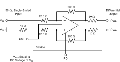 Figure 54. Single-Ended Input to Differential Output Amplifier
9.3.2.1 Resistor Design Equations for Single-to-Differential Applications
Even though the resistors for the LMH3401 are on-chip, being familiar with the FDA resistor selection criteria is still important. The design equations for setting the resistors around an FDA to convert from a single-ended input signal to a differential output can be approached in several ways. In this section, several critical assumptions are made to simplify the results:
- The feedback resistors are selected first and set to be equal on the two sides of the device.
- The dc and ac impedances from the summing junctions back to the signal source and ground (or a bias voltage on the non-signal input side) are set as equal to retain the feedback divider balance on each side of the FDA.
Both of these assumptions are typical and aimed to deliver the best dynamic range through the FDA signal path.
After the feedback resistor values are chosen, the aim is to solve for RT (a termination resistor to ground on the signal input side), RG1 (the input gain resistor for the signal path), and RG2 (the matching gain resistor on the non-signal input side), as shown in Figure 55 (this example uses the THS4541, an external resistor FDA). The same resistor solutions can be applied to either ac- or dc-coupled paths. Adding blocking capacitors in the input-signal chain is a simple option. Adding these blocking capacitors after the RT element (as shown in Figure 55) has the advantage of removing any dc currents in the feedback path from the output VOCM to ground.
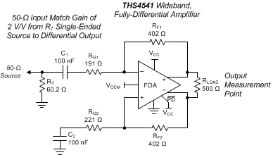 Figure 55. AC-Coupled, Single-Ended Source to a Differential Gain of a 2-V/V Test Circuit
Most FDA amplifiers use external resistors and have complete flexibility in the selected RF, just like the THS4541 does in Figure 55, however the LMH3401 has on-chip feedback resistors that are fixed at 200 Ω. The equations used in this section still apply, and an external resistance can be added to the on-chip RG resistors.
After the feedback resistor values are chosen, the aim is to solve for RT (a termination resistor to ground on the signal input side), RG1 (the input gain resistor for the signal path), and RG2 (the matching gain resistor on the non-signal input side). The same resistor solutions can be applied to either ac- or dc-coupled paths. Adding blocking capacitors in the input-signal chain is a simple option. Adding these blocking capacitors after the RT element has the advantage of removing any dc currents in the feedback path from the output VOCM to ground.
Earlier approaches to the solutions for RT and RG1 (when the input must be matched to a source impedance, RS) follow an iterative approach. This complexity arises from the active input impedance at the RG1 input. When the FDA is used to convert a single-ended signal to differential, the common-mode input voltage at the FDA inputs must move with the input signal to generate the inverted output signal as a current in the RG2 element. A more recent solution is illustrated in Equation 2, where a quadratic in RT can be solved for an exact required value. This quadratic emerges from the simultaneous solution for a matched input impedance and target gain. The only inputs required are:
- The selected RF value.
- The target voltage gain (AV) from the input of RT to the differential output voltage.
- The desired input impedance at the junction of RT and RG1 to match RS.
Solving this quadratic for RT starts the solution sequence, as shown in Equation 2:
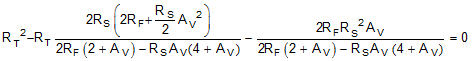
Being a quadratic, there are limits to the range of solutions. Specifically, after RF and RS are chosen, there is physically a maximum gain beyond which Equation 2 starts to solve for negative RT values (if input matching is a requirement). With RF selected, use Equation 3 to verify that the maximum gain is greater than the desired gain.
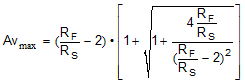
If the achievable AVmax is less than desired, increase the RF value. After RT is derived from Equation 2, the RG1 element is given by Equation 4:
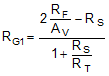
Then, the simplest approach is to use a single RG2 = RT || RS + RG1 on the non-signal input side. Often, this approach is shown as the separate RG1 and RS elements. This approach can provide a better divider match on the two feedback paths, but a single RG2 is often acceptable. A direct solution for RG2 is given as Equation 5:

This design proceeds from a target input impedance matched to RS, signal gain AV, and a selected RF value. The nominal RF value chosen for the LMH3401 characterization is 200 Ω. As discussed previously, this resistance is on-chip and cannot be changed.
Note that when driving the LMH3401 with a 50-Ω source impedance the on-chip resistor is RG1 and the other input requires only 50 Ω to complete RG2. The above equations are provided to help show the effects of the active termination and to assist when using the LMH3401 with source impedances other than 50 Ω.
9.3.2.2 Input Impedance Calculations
The designs so far have included a source impedance, RS, that must be matched by RT and RG1. The total impedance with respect to the input at RG1 for the circuit of Figure 54 is the parallel combination of RT to ground and ZA (active impedance) presented by the amplifier input at RG1. That expression, assuming RG2 is set to obtain a differential divider balance, is given by Equation 6:
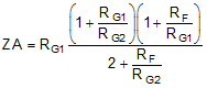
For designs that do not need impedance matching (but instead come from the low-impedance output of another amplifier, for instance), RG1 = RG2 is the single-to-differential design used without RT to ground. Setting RG1 = RG2 = RG in Equation 6 gives the input impedance of a simple input FDA driving from a low-impedance, single-ended source to a differential output.
9.3.3 Differential to Differential Signals
The LMH3401 can also be used to amplify differential input signals to differential output signals. A basic block diagram of the circuit is shown in Figure 56. The differential input impedance set by the on-chip resistors is lower than optimal for most applications (25 Ω). In order to match a load such as 100 Ω, external resistors are required, as shown in Figure 57.
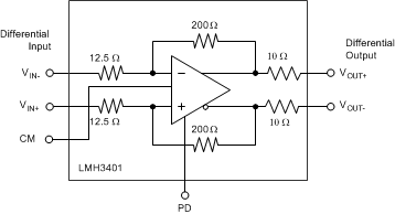 Figure 56. Differential Input To Differential Output Amplifier
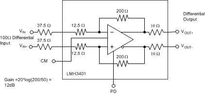 Figure 57. Differential Input Configured for a 100-Ω Source
9.3.4 Output Common-Mode Voltage
The CM input controls the output common-mode voltage. CM has no internal biasing network and must be driven by an external source or resistor divider network to the positive power supply. The CM input impedance is very high and bias current is not critical. Also, the CM input has no internal reference and must be driven from an external source. Using a bypass capacitor is also necessary. A capacitor value of 0.01 µF is recommended. For best harmonic distortion, maintain the CM input within ±1 V of the mid-supply voltage using a 5-V supply and within ±0.5 V when using a 3.3-V supply. The CM input voltage can be operated outside this range if lower output swing is used or distortion degradation is allowed. For more information, see Figure 18 and Figure 19.
9.4 Device Functional Modes
9.4.1 Operation with a Split Supply
The LMH3401 can be operated using split supplies. One of the most common supply configurations is ±2.5 V. In this case, VS+ is connected to 2.5 V, and VS– is connected to –2.5 V, while the GND pins are connected to the system ground. As with any device, the LMH3401 is impervious to what the levels are named in the system. In essence, using split supplies is simply a level shift of the power pins by –2.5 V. If everything else is level-shifted by the same amount, the device does not detect any difference. With a ±2.5-V power supply, the CM range is
0 V ±1 V; while the input has a slightly larger range of –2.5 V to 1 V; see Figure 22. This design has certain advantages in systems where signals are referenced to ground, and as noted in the ADC Input Common-Mode Voltage Considerations—DC-Coupled Input section, for driving ADCs with low input common-mode voltage requirements in dc-coupled applications. With the GND pin connected to the system ground, the power-down threshold is 1.2 V which is compatible with most logic levels from 1.5-V CMOS to 2.5-V CMOS.
As noted previously, the absolute supply voltage values are not critical. For example, using a 4-V VS+ and a
–1-V VS– is still a 5-V supply condition. As long as the input and output common-mode voltages remain in the optimum range, the amplifier can operate on any supply voltages from 3.3 V to 5.25 V. When considering using supply voltages near the 3.3-V total supply, be very careful to make sure that the amplifier performance is adequate. Setting appropriate common-mode voltages for large-signal swing conditions becomes difficult when the supply voltage is below 4 V.
9.4.2 Operation with a Single Supply
As with split supplies, the LMH3410 can be operated from single-supply voltages from 3.3 V to 5.25 V. Single-supply operation is most appropriate when the signal path is ac coupled and the input and output common-mode voltages are set to mid supply by the CM pin and are preserved by coupling capacitors on the input and output. For example, with a single 5-V supply the amplifier outputs are biased to between 2.0 V and 3.0 V. The input common-mode range is more forgiving towards the negative supply rail, thus the input voltage can range from
0 V to 3.5 V. Although the amplifier operates outside these recommendations, there is less signal swing available and performance degrades.