SNLS309I April 2010 – December 2014 LMH1983
PRODUCTION DATA.
- 1 Features
- 2 Applications
- 3 Description
- 4 Revision History
- 5 Description (continued)
- 6 Pin Configurations and Functions
- 7 Specifications
-
8 Detailed Description
- 8.1 Overview
- 8.2 Functional Block Diagram
- 8.3
Feature Description
- 8.3.1 Control of PLL1
- 8.3.2 PLL1 Loop Response Design Equations
- 8.3.3 Control of PLL2 and PLL3
- 8.3.4 Control of PLL4
- 8.3.5 Clock Output Jitter
- 8.3.6 Lock Determination
- 8.3.7 Lock Time Considerations
- 8.3.8 LOR Determination
- 8.3.9 Output Driver Adjustments
- 8.3.10 TOF1 Alignment
- 8.3.11 TOF2 and TOF3 Alignment
- 8.3.12 TOF4 Alignment
- 8.4 Device Functional Modes
- 8.5 Programming
- 8.6 Register Map
- 9 Applications and Implementation
- 10Power Supply Recommendations
- 11Layout
- 12Device and Documentation Support
- 13Mechanical, Packaging, and Orderable Information
1 Features
- Four PLLs for Simultaneous A/V Clock Generation
- PLL1: 27 or 13.5 MHz
- PLL2: 148.5 or 74.25 MHz
- PLL3: 148.5/1.001 or 74.25/1.001 MHz
- PLL4: 98.304 MHz / 2X (X = 0 to 15)
- 3 x 2 Video Clock Crosspoint
- Flexible PLL Bandwidth to Optimize Jitter Performance and Lock Time
- Soft Resynchronization to New Reference
- Digital Holdover or Free-run on Loss of Reference
- Status Flags for Loss of Reference and Loss of PLL Lock
- 3.3 V Single Supply Operation
- I2C Interface with Address Select Pin (3 States)
2 Applications
- Triple Rate (3G/HD/SD) SDI SerDes
- FPGA Reference Clock Generation/Cleaning
- Audio Embed or De-embed
- Video Cameras
- Frame Synchronizers (Genlock, DARS)
- A-D or D-A Conversion, Editing, Processing Cards
- Keyers and Logo Inserters
- Format or Standards Converters
- Video Displays and Projectors
- A/V Test and Measurement Equipment
3 Description
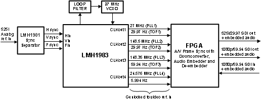
The LMH1983 is a highly-integrated programmable audio/video (A/V) clock generator intended for broadcast and professional applications. It can replace multiple PLLs and VCXOs used in applications supporting SMPTE serial digital video (SDI) and digital audio AES3/EBU standards. It offers low-jitter reference clocks for any SDI transmitter to meet stringent output jitter specifications without additional clock cleaning circuits.
The LMH1983 features automatic input format detection, simple programming of multiple A/V output formats, genlock or digital free-run modes, and override programmability of various automatic functions. The recognized input formats include HVF syncs for the major video standards, 27 MHz, 10 MHz, and 32/44.1/48/96 kHz audio word clocks.
The dual-stage PLL architecture integrates four PLLs with three on-chip VCOs. The first stage (PLL1) uses an external low-noise 27 MHz VCXO with narrow loop bandwidth to provide a clean reference clock for the next stage. The second stage (PLL2, 3, 4) consists of three parallel VCO PLLs for simultaneous generation of the major digital A/V clock fundamental rates, including 148.5 MHz, 148.5/1.001 MHz, and 98.304 MHz (4 × 24.576 MHz). Each PLL can generate a clock and a timing pulse to indicate top of frame (TOF).
Device Information(1)
| PART NUMBER | PACKAGE | BODY SIZE (NOM) |
|---|---|---|
| LMH1983 | WQFN (40) | 6.00 mm × 6.00 mm |
- For all available packages, see the orderable addendum at the end of the datasheet.
Typical Application Block Diagram