ZHCSID0D April   2016  – June 2018 LMH1226

PRODUCTION DATA.  

  1. 特性
  2. 应用
  3. 说明
    1.     Device Images
      1.      简化框图
  4. 修订历史记录
  5. Pin Configuration and Functions
    1.     Pin Functions
  6. Specifications
    1. 6.1 Absolute Maximum Ratings
    2. 6.2 ESD Ratings
    3. 6.3 Recommended Operating Conditions
    4. 6.4 Thermal Information
    5. 6.5 Electrical Characteristics
    6. 6.6 Recommended SMBus Interface AC Timing Specifications
    7. 6.7 Serial Parallel Interface (SPI) AC Timing Specifications
    8. 6.8 Typical Characteristics
  7. Detailed Description
    1. 7.1 Overview
    2. 7.2 Functional Block Diagram
    3. 7.3 Feature Description
      1. 7.3.1 4-Level Input Configuration Pins
      2. 7.3.2 Input Carrier Detect
      3. 7.3.3 Continuous Time Linear Equalizer (CTLE)
        1. 7.3.3.1 Adaptive PCB Trace Equalizer (IN1±)
      4. 7.3.4 Input-Output Mux Selection
      5. 7.3.5 Clock and Data Recovery (CDR) Reclocker
      6. 7.3.6 Internal Eye Opening Monitor (EOM)
      7. 7.3.7 Output Function Control
      8. 7.3.8 Output Driver Amplitude and De-Emphasis Control
      9. 7.3.9 Status Indicators and Interrupts
        1. 7.3.9.1 LOCK_N (Lock Indicator)
        2. 7.3.9.2 CD_N (Carrier Detect)
        3. 7.3.9.3 INT_N (Interrupt)
    4. 7.4 Device Functional Modes
      1. 7.4.1 System Management Bus (SMBus) Mode
        1. 7.4.1.1 SMBus Read and Write Transactions
          1. 7.4.1.1.1 SMBus Write Operation Format
          2. 7.4.1.1.2 SMBus Read Operation Format
      2. 7.4.2 Serial Peripheral Interface (SPI) Mode
        1. 7.4.2.1 SPI Read and Write Transactions
          1. 7.4.2.1.1 SPI Write Transaction Format
          2. 7.4.2.1.2 SPI Read Transaction Format
        2. 7.4.2.2 SPI Daisy Chain
    5. 7.5 LMH1226 Register Map
      1. 7.5.1 Share Register Page
      2. 7.5.2 CTLE/CDR Register Page
      3. 7.5.3 Drivers Register Page
  8. Application and Implementation
    1. 8.1 Application Information
      1. 8.1.1 General Guidance for SMPTE and 10 GbE Applications
      2. 8.1.2 LMH1219 and LMH1226 Compatibility
    2. 8.2 Typical Application
      1. 8.2.1 Design Requirements
      2. 8.2.2 Detailed Design Procedure
      3. 8.2.3 Recommended VOD and DEM Register Settings
      4. 8.2.4 Application Performance Plots
  9. Power Supply Recommendations
  10. 10Layout
    1. 10.1 PCB Layout Guidelines
    2. 10.2 Layout Example
  11. 11器件和文档支持
    1. 11.1 接收文档更新通知
    2. 11.2 社区资源
    3. 11.3 商标
    4. 11.4 静电放电警告
    5. 11.5 术语表
  12. 12机械、封装和可订购信息

封装选项

机械数据 (封装 | 引脚)
散热焊盘机械数据 (封装 | 引脚)
订购信息

Application Performance Plots

The LMH1226 performance was measured with the test setup shown in Figure 22.

LMH1226 app_test_setup_diagram_IN1.gifFigure 22. Test Setup for LMH1226 PCB Equalizer (IN1±)

The eye diagrams in this subsection show how the LMH1226 improves overall signal integrity in the data path for 100-Ω differential FR4 PCB trace at IN1.
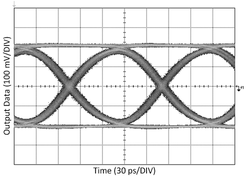
LMH1226 IN1_10GbE_20in5mil_100mvDIV_30psDIV_EQonly_manual1100.gif
VOD_DE = H, IN_OUT_SEL = L, OUT_CTRL = L
Figure 23. 10.3125 Gbps, TL = 20 in. 5-Mil FR4, EQ Only
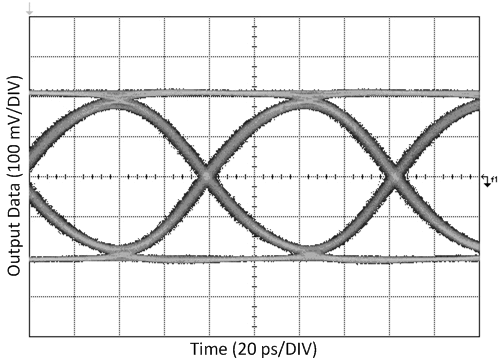
LMH1226 IN1_12G_20in5mil_100mvDIV_20psDIV_EQonly_manual1100.gif
VOD_DE = H, IN_OUT_SEL = H, OUT_CTRL = L
Figure 25. 11.88 Gbps, TL = 20 in. 5-Mil FR4, EQ Only
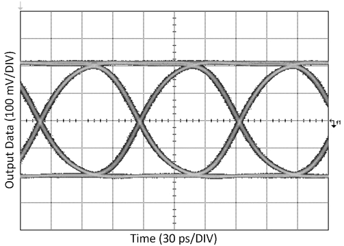
LMH1226 IN1_10GbE_20in5mil_100mvDIV_30psDIV_Retimed.gif
VOD_DE = H, IN_OUT_SEL = L, OUT_CTRL = F
Figure 24. 10.3125 Gbps, TL = 20 in. 5-Mil FR4, Reclocked
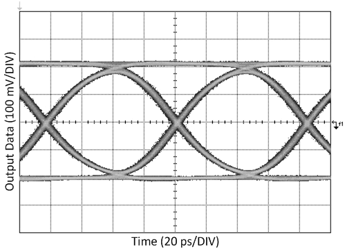
LMH1226 IN1_12G_20in5mil_100mvDIV_20psDIV_Retimed.gif
VOD_DE = H, IN_OUT_SEL = H, OUT_CTRL = F
Figure 26. 11.88 Gbps, TL = 20 in. 5-Mil FR4, Reclocked