SNLS308G April 2009 – June 2015 LMH0384
PRODUCTION DATA.
- 1 Features
- 2 Applications
- 3 Description
- 4 Revision History
- 5 Pin Configuration and Functions
- 6 Specifications
- 7 Detailed Description
- 8 Application and Implementation
- 9 Power Supply Recommendations
- 10Layout
- 11Device and Documentation Support
- 12Mechanical, Packaging, and Orderable Information
8 Application and Implementation
NOTE
Information in the following applications sections is not part of the TI component specification, and TI does not warrant its accuracy or completeness. TI’s customers are responsible for determining suitability of components for their purposes. Customers should validate and test their design implementation to confirm system functionality.
8.1 Application Information
The LMH0384 is a single-channel, 3-Gbps HD - SD SDI Adaptive Cable Equalizer designed to equalize data transmitted over cable or any media with similar dispersive loss characteristics. The equalizer operates over a wide range of data rates from 125 Mbps to 2.97 Gbps and supports ST 424, ST 292, ST 344, and ST 259. Additional features include separate carrier detect and output mute pins which may be tied together to mute the output when no signal is present. A programmable mute reference is provided to mute the output at a selectable level of signal degradation. The bypass pin allows the adaptive equalizer to be bypassed. The LMH0384 accepts either a differential or single-ended input. The input must be AC-coupled.
The LMH0384 correctly handles equalizer pathological signals for standard definition and high definition serial digital video, as described in ST RP 178 and RP 198, respectively.
8.1.1 Replacing the LMH0344
In pin mode, the LMH0384 is a drop-in replacement for the LMH0344SQ SDI cable equalizer. When replacing an LMH0344 with an LMH0384, it is important to consider the following points:
- The LMH0384 auto sleep function is mapped to pin 12 which is a ground pin on the LMH0344SQ. When this pin is grounded on the LMH0384, the auto sleep function is disabled. To enable auto sleep mode on the LMH0384, pin 12 must be pulled high.
- Pin 4 and pin 9 on the LMH0344SQ are true ground pins. For the LMH0384, pin 4 and pin 9 may be driven logic low in pin mode (they do not require a true ground connection).
- The LMH0384 has lower input capacitance than the LMH0344 which allows for improved input return loss. The input return loss network may need to be modified. In most cases, the LMH0384 should provide superior input return loss.
- The LMH0384 default output common-mode voltage is different than that of the LMH0344. In most cases, this should not cause an issue. The LMH0384 and LMH0344 outputs can both be DC coupled to TI's SDI reclockers and cable drivers. In addition, the LMH0384 output can be DC coupled to LVDS and other inputs that require lower input common-mode voltages than the LMH0344. The LMH0384 output common-mode voltage is adjustable through the SPI.
8.2 Typical Application
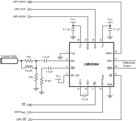
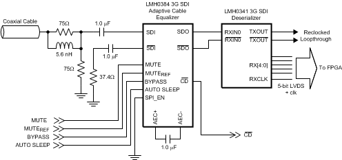
Figure 11 and Figure 12 show the application circuit for the LMH0384 in SPI mode and Pin mode.
 Figure 11. Application Circuit (SPI Mode)
 Figure 12. Typical Application (Pin Mode)
8.2.1 Design Requirements
Table 2 lists the design parameters for the LMH0384.
Table 2. LMH0384 Design Parameters
| DESIGN PARAMETER | REQUIREMENT |
|---|---|
| Input AC-coupling capacitors | Required. A common type of AC-coupling capacitor is 1 µF ±10% X7R ceramic capacitor (0402 or 0201 size). Capacitors may be implemented on the PCB or in the connector. |
| Output AC-coupling capacitors | The user should check input common mode voltage. If AC coupling capacitor is required, SDO AC-coupling capacitor is expected to be 4.7 µF ±10%. |
| Distance from Device to BNC | Keep this distance as short as possible to minimize parasitic |
| Input launch amplitude | Refer to DC Electrical Characteristics |
8.2.2 Detailed Design Procedure
- Maximum power draw for PCB regulator selection. For this use maximum power consumption in the data sheet.
- Closely compare schematic against typical connection diagram in the data sheet.
- Plan out the PCB layout and component placement to minimize parasitic.
- Consult the BNC vendor for optimum BNC landing pattern.
8.3 Dos and Don'ts
Pay special attention to the PCB layout for the high speed signals. The SMPTE specifies the requirements for the Serial Digital Interface to transport digital video at SD, HD, and 3 Gbps data rates over coaxial cables. One of the requirements is meeting the required Return Loss. This requirement specifies how closely the port resembles 75-Ω impedance across a specified frequency band. The SMPTE specifications also defines the use of AC-coupling capacitors for transporting uncompressed serial data streams with heavy low frequency content. This specification requires the use of a 1-µF AC-coupling capacitors on the input of the LMH0384 to avoid low frequency DC wander.

