ZHCSAK2H April 2007 – June 2016 LMH0302
PRODUCTION DATA.
7 Detailed Description
7.1 Overview
The LMH0302 ST 424, ST292, ST259 serial digital cable driver is a monolithic, high-speed cable driver designed for use in serial digital video data transmission applications. The LMH0302 drives 75-Ω transmission lines (Belden 8281, 1694A, Canare L-5CFB, or equivalent) at data rates up to 2.97 Gbps.
The LMH0302 provides two selectable slew rates for ST 259 and ST 292/424 compliance. The output voltage swing is adjustable through a single external resistor ( RREF).
The LMH0302 is powered from a single 3.3-V supply. Power consumption is typically 125 mW in SD mode and 165 mW in HD mode. The LMH0302 is available in a 16-pin WQFN package.
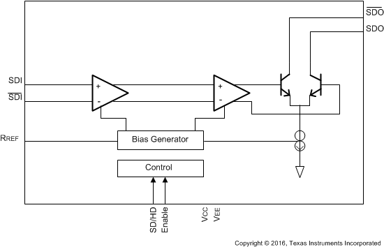
7.2 Functional Block Diagram

7.3 Feature Description
The LMH0302 data path consists of several key blocks:
- Input interfacing
- Output interfacing
- Output slew rate control
- Output enable
7.3.1 Input Interfacing
The LMH0302 accepts either differential or single-ended input. The inputs are self-biased, allowing for simple AC or DC coupling. DC-coupled inputs must be kept within the specified common-mode range.
7.3.2 Output Interfacing
The LMH0302 uses current mode outputs. Single-ended output levels are 800 mVP-P into 75-Ω AC-coupled coaxial cable with an RREF resistor of 750 Ω. The RREF resistor is connected between the RREF pin and VCC.
The RREF resistor must be placed as close as possible to the RREF pin. In addition, the copper in the plane layers below the RREF network must be removed to minimize parasitic capacitance.
7.3.3 Output Slew Rate Control
The LMH0302 output rise and fall times are selectable for either ST 259, ST 424, or 292 compliance through the SD/HD pin. For slower rise and fall times, or ST 259 compliance, SD/HD is set high. For faster rise and fall times, ST 424 and ST 292 compliance, SD/HD is set low.
7.3.4 Output Enable
The SDO/SDO output driver are enabled or disabled with the ENABLE pin. When set low, the output driver is powered off. ENABLE has an internal pullup.
7.4 Device Functional Modes
The LMH0302 features are programmed using pin mode only.