ZHCSAK2H April 2007 – June 2016 LMH0302
PRODUCTION DATA.
6 Specifications
6.1 Absolute Maximum Ratings
over operating free-air temperature range (unless otherwise noted)(1)| MIN | MAX | UNIT | ||
|---|---|---|---|---|
| Supply voltage | –0.5 | 3.6 | V | |
| Input voltage (all inputs) | –0.3 | VCC + 0.3 | V | |
| Output current | 28 | mA | ||
| Lead temperature, soldering (4 s) | 260 | °C | ||
| Junction temperature, TJ | 125 | °C | ||
| Storage temperature, Tstg | –65 | 150 | °C | |
(1) Stresses beyond those listed under Absolute Maximum Ratings may cause permanent damage to the device. These are stress ratings only, which do not imply functional operation of the device at these or any other conditions beyond those indicated under Recommended Operating Conditions. Exposure to absolute-maximum-rated conditions for extended periods may affect device reliability.
6.2 ESD Ratings
| VALUE | UNIT | |||
|---|---|---|---|---|
| V(ESD) | Electrostatic discharge | Human-body model (HBM), per ANSI/ESDA/JEDEC JS-001(1) | ±4500 | V |
| Charged-device model (CDM), per JEDEC specification JESD22-C101(2) | ±2000 | |||
| Machine model (MM) | ±250 | |||
(1) JEDEC document JEP155 states that 500-V HBM allows safe manufacturing with a standard ESD control process.
(2) JEDEC document JEP157 states that 250-V CDM allows safe manufacturing with a standard ESD control process.
6.3 Recommended Operating Conditions
over operating free-air temperature range (unless otherwise noted)| MIN | NOM | MAX | UNIT | ||
|---|---|---|---|---|---|
| Supply voltage (VCC – VEE) | 3.13 | 3.3 | 3.46 | V | |
| Operating junction temperature | 100 | °C | |||
| Operating free air temperature, TA | –40 | 25 | 85 | °C | |
6.4 Thermal Information
| THERMAL METRIC(1) | LMH0302 | UNIT | |
|---|---|---|---|
| RUM (WQFN) | |||
| 16 PINS | |||
| RθJA | Junction-to-ambient thermal resistance | 47.8 | °C/W |
| RθJC(top) | Junction-to-case (top) thermal resistance | 47.2 | °C/W |
| RθJB | Junction-to-board thermal resistance | 25.6 | °C/W |
| ψJT | Junction-to-top characterization parameter | 1.7 | °C/W |
| ψJB | Junction-to-board characterization parameter | 25.7 | °C/W |
| RθJC(bot) | Junction-to-case (bottom) thermal resistance | 14.5 | °C/W |
(1) For more information about traditional and new thermal metrics, see the Semiconductor and IC Package Thermal Metrics application report, SPRA953.
6.5 Electrical Characteristics – DC
Over supply voltage and operating free-air temperature range (unless otherwise noted) (1)(2)| PARAMETER | TEST CONDITIONS | MIN | TYP | MAX | UNIT | |
|---|---|---|---|---|---|---|
| VCMIN | Input common mode voltage | SDI, SDI | 1.1 + VSDI/2 | VCC – VSDI/2 | V | |
| VSDI | Input voltage swing | Differential, SDI, SDI | 100 | 2200 | mVP−P | |
| VCMOUT | Output common mode voltage | SDO, SDO | VCC – VSDO | V | ||
| VSDO | Output voltage swing | Single-ended, 75-Ω load, RREF = 750 Ω 1% |
720 | 800 | 880 | mVP−P |
| VIH | Input voltage high level | SD/HD, ENABLE | 2 | V | ||
| VIL | Input voltage low level | SD/HD, ENABLE | 0.8 | V | ||
| ICC | Supply current | SD/HD = 0, SDO/SDO enabled | 50 | 59 | mA | |
| SD/HD = 0, SDO/SDO disabled | 26 | 33 | ||||
| SD/HD = 1, SDO/SDO enabled | 38 | 48 | ||||
| SD/HD = 1, SDO/SDO disabled | 15 | 22 | ||||
(1) Current flow into device pins is defined as positive. Current flow out of device pins is defined as negative. All voltages are stated referenced to VEE = 0 V.
(2) Typical values are stated for VCC = 3.3 V and TA = 25°C.
6.6 Electrical Characteristics – AC
Over supply voltage and operating free-air temperature range (unless otherwise noted) (1)| PARAMETER | TEST CONDITIONS | MIN | TYP | MAX | UNIT | |
|---|---|---|---|---|---|---|
| DRSDI | Input data rate | SDI, SDI | 2970 | Mbps | ||
| Tjit | Additive jitter | 2.97 Gbps, SDO, SDO | 20 | psP-P | ||
| 1.485 Gbps, SDO, SDO | 18 | |||||
| 270 Mbps, SDO, SDO | 15 | |||||
| tr,tf | Output rise time, fall time | SD/HD = 0, 20% – 80%, SDO, SDO | 90 | 130 | ps | |
| SD/HD = 1, 20% – 80%, SDO, SDO | 400 | 800 | ||||
| TMATCH | Mismatch in rise time, fall time | SD/HD = 0, SDO, SDO | 30 | ps | ||
| SD/HD = 1, SDO, SDO | 50 | |||||
| TDCD | Duty cycle distortion | SD/HD = 0, 2.97 Gbps, SDO, SDO(2) | 27 | ps | ||
| SD/HD = 0, 1.485 Gbps, SDO, SDO(2) | 30 | |||||
| SD/HD = 1, SDO, SDO(2) | 100 | |||||
| TOS | Output overshoot | SD/HD = 0, SDO, SDO(2) | 10% | |||
| SD/HD = 1, SDO, SDO(2) | 8% | |||||
| RLSDO | Output return loss | 5 MHz to 1.5 GHz, SDO, SDO(3) | 15 | dB | ||
| 1.5 GHz to 3.0 GHz, SDO, SDO(3) | 10 | |||||
(1) Typical values are stated for VCC = 3.3 V and TA = 25°C.
(2) Specification is ensured by characterization.
(3) Output return loss is dependent on board design. The LMH0302 meets this specification on the SD302 evaluation board.
6.7 Typical Characteristics
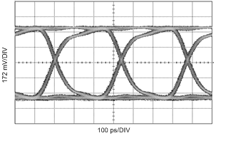
Typical device characteristics at TA = 25°C and VCC = 3.3 V (unless otherwise noted) Figure 1. SDO PRBS10 at 2.97 Gbps
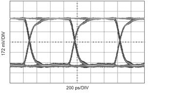
 Figure 2. SDO PRBS10 at 1.485 Gbps