ZHCSFT3D March   2015  – March 2017 LMG5200

PRODUCTION DATA.  

  1. 特性
  2. 应用
  3. 说明
  4. 修订历史记录
  5. Pin Configuration and Functions
  6. Specifications
    1. 6.1 Absolute Maximum Ratings
    2. 6.2 ESD Ratings
    3. 6.3 Recommended Operating Conditions
    4. 6.4 Thermal Information
    5. 6.5 Electrical Characteristics
    6. 6.6 Typical Characteristics
  7. Parameter Measurement Information
    1. 7.1 Propagation Delay and Mismatch Measurement
  8. Detailed Description
    1. 8.1 Overview
    2. 8.2 Functional Block Diagram
    3. 8.3 Feature Description
      1. 8.3.1 Control Inputs
      2. 8.3.2 Start-up and UVLO
      3. 8.3.3 Bootstrap Supply Voltage Clamping
      4. 8.3.4 Level Shift
    4. 8.4 Device Functional Modes
  9. Application and Implementation
    1. 9.1 Application Information
    2. 9.2 Typical Application
      1. 9.2.1 Design Requirements
      2. 9.2.2 Detailed Design Procedure
        1. 9.2.2.1 VCC Bypass Capacitor
        2. 9.2.2.2 Bootstrap Capacitor
        3. 9.2.2.3 Power Dissipation
      3. 9.2.3 Application Curves
  10. 10Power Supply Recommendations
  11. 11Layout
    1. 11.1 Layout Guidelines
    2. 11.2 Layout Examples
  12. 12器件和文档支持
    1. 12.1 器件支持
      1. 12.1.1 开发支持
    2. 12.2 文档支持
      1. 12.2.1 相关文档
    3. 12.3 接收文档更新通知
    4. 12.4 社区资源
    5. 12.5 商标
    6. 12.6 静电放电警告
    7. 12.7 Glossary
  13. 13机械、封装和可订购信息
    1. 13.1 封装信息

封装选项

机械数据 (封装 | 引脚)
散热焊盘机械数据 (封装 | 引脚)
订购信息

Pin Configuration and Functions

MOF Package
9-Pin QFM
Top View
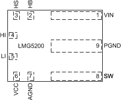
LMG5200 pinout_mof_9_snoscy4.gif

Pin Functions

PIN I/O(1) DESCRIPTION
NAME NO.
AGND 7 G Analog ground. Ground of driver device.
HB 2 P High-side gate driver bootstrap rail.
HI 4 I High-side gate driver control input
HS 3 P High-side GaN FET source connection
LI 5 I Low-side driver control input
PGND 9 G Power ground. Low-side GaN FET source. Electrically shorted to AGND pin.
SW 8 P Switching node. Electrically shorted to HS pin. Ensure low capacitance at this node on PCB.
VCC 6 P 5-V positive gate drive supply
VIN 1 P Input voltage pin. Electrically connected to high-side GaN FET drain.
I = Input, O = Output, G = Ground, P = Power