ZHCSFT3D March 2015 – March 2017 LMG5200
PRODUCTION DATA.
11 Layout
11.1 Layout Guidelines
To maximize the efficiency benefits of fast switching, it is extremely important to optimize the board layout such that the power loop impedance is minimal. When using a multilayer board (more than 2 layers), power loop parasitic impedance is minimized by having the return path to the input capacitor (between VIN and PGND), small and directly underneath the first layer as shown in Figure 14 and Figure 15. Loop inductance is reduced due to flux cancellation as the return current is directly underneath and flowing in the opposite direction. It is also critical that the VCC capacitors and the bootstrap capacitors are as close as possible to the device and in the first layer. Carefully consider the AGND connection of LMG5200 device. It must NOT be directly connected to PGND so that PGND noise does not directly shift AGND and cause spurious switching events due to noise injected in HI and LI signals.
11.2 Layout Examples
Placements shown in Figure 14 and in the cross section of Figure 15 show the suggested placement of the device with respect to sensitive passive components, such as VIN, bootstrap capacitors (HS and HB) and VSS capacitors. Use appropriate spacing in the layout to reduce creepage and maintain clearance requirements in accordance with the application pollution level. Inner layers if present can be more closely spaced due to negligible pollution.
The layout must be designed to minimize the capacitance at the SW node. Use as small an area of copper as possible to connect the device SW pin to the inductor, or transformer, or other output load. Furthermore, ensure that the ground plane or any other copper plane has a cutout so that there is no overlap with the SW node, as this would effectively form a capacitor on the printed circuit board. Additional capacitance on this node reduces the advantages of the advanced packaging approach of the LMG5200 and may result in reduced performance. Figure 16, Figure 17, Figure 18, and Figure 19 show an example of how to design for minimal SW node capacitance on a four-layer board. In these figures, U1 is the LMG5200 device.
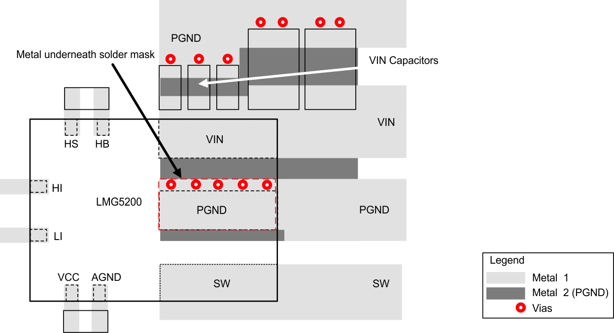 Figure 14. External Component Placement (Single Layer)
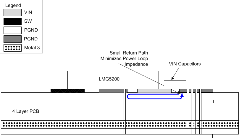 Figure 15. Four-Layer Board Cross Section With Return Path Directly Underneath for Power Loop
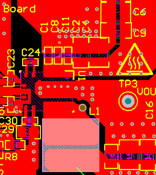 Figure 16. Top Layer
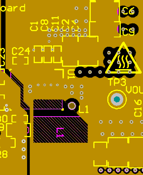 Figure 18. Middle Layer
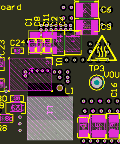 Figure 17. Ground Plane
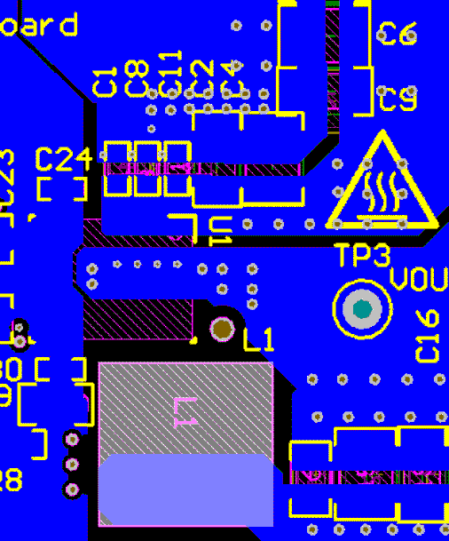 Figure 19. Bottom Layer
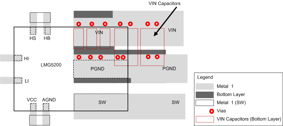 Figure 20. External Component Placement (Double Layer PCB)
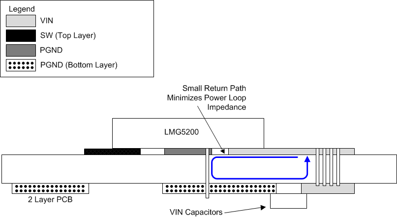 Figure 21. Two-Layer Board Cross Section With Return Path
Two-layer boards are not recommended for use with LMG5200 device due to the larger power loop inductance. However, if design considerations allow only two board layers, place the input decoupling capacitors immediately behind the device on the back-side of the board to minimize loop inductance. Figure 20 and Figure 21 show a layout example for two-layer boards.