SNIS153D July   2009  – October 2015 LM75B

PRODUCTION DATA.  

  1. Features
  2. Applications
  3. Description
  4. Revision History
  5. Pin Configuration and Functions
  6. Specifications
    1. 6.1 Absolute Maximum Ratings
    2. 6.2 ESD Ratings
    3. 6.3 Recommended Operating Conditions
    4. 6.4 Thermal Information
    5. 6.5 Temperature-to-Digital Converter Characteristics
    6. 6.6 Digital DC Characteristics
    7. 6.7 I2C Digital Switching Characteristics
    8. 6.8 Typical Characteristics
  7. Detailed Description
    1. 7.1 Overview
    2. 7.2 Functional Block Diagram
    3. 7.3 Feature Description
      1. 7.3.1 Digital Temperature Sensor
    4. 7.4 Device Functional Modes
    5. 7.5 Programming
      1. 7.5.1 I2C Bus Interface
      2. 7.5.2 Temperature Data Format
      3. 7.5.3 Shutdown Mode
      4. 7.5.4 Fault Queue
      5. 7.5.5 Comparator and Interrupt Mode
      6. 7.5.6 O.S. Output
      7. 7.5.7 O.S. Polarity
      8. 7.5.8 Internal Register Structure
    6. 7.6 Register Maps
      1. 7.6.1 Pointer Register (Selects Which Registers Will Be Read From or Written to):
      2. 7.6.2 Temperature Register (Read Only):
      3. 7.6.3 Configuration Register (Read/Write):
      4. 7.6.4 THYST and TOS Register (Read/Write):
  8. Application and Implementation
    1. 8.1 Application Information
    2. 8.2 Typical Application
      1. 8.2.1 Simple Fan Controller, Interface Optional
        1. 8.2.1.1 Design Requirements
        2. 8.2.1.2 Detailed Design Procedure
        3. 8.2.1.3 Application Curve
    3. 8.3 System Examples
      1. 8.3.1 Simple Thermostat, Interface Optional
      2. 8.3.2 Temperature Sensor with Loudmouth Alarm (Barking Watchdog)
  9. Power Supply Recommendations
  10. 10Layout
    1. 10.1 Layout Guidelines
      1. 10.1.1 Digital Noise Issues
    2. 10.2 Layout Example
  11. 11Device and Documentation Support
    1. 11.1 Related Links
    2. 11.2 Community Resources
    3. 11.3 Trademarks
    4. 11.4 Electrostatic Discharge Caution
    5. 11.5 Glossary
  12. 12Mechanical, Packaging, and Orderable Information

封装选项

机械数据 (封装 | 引脚)
散热焊盘机械数据 (封装 | 引脚)
订购信息

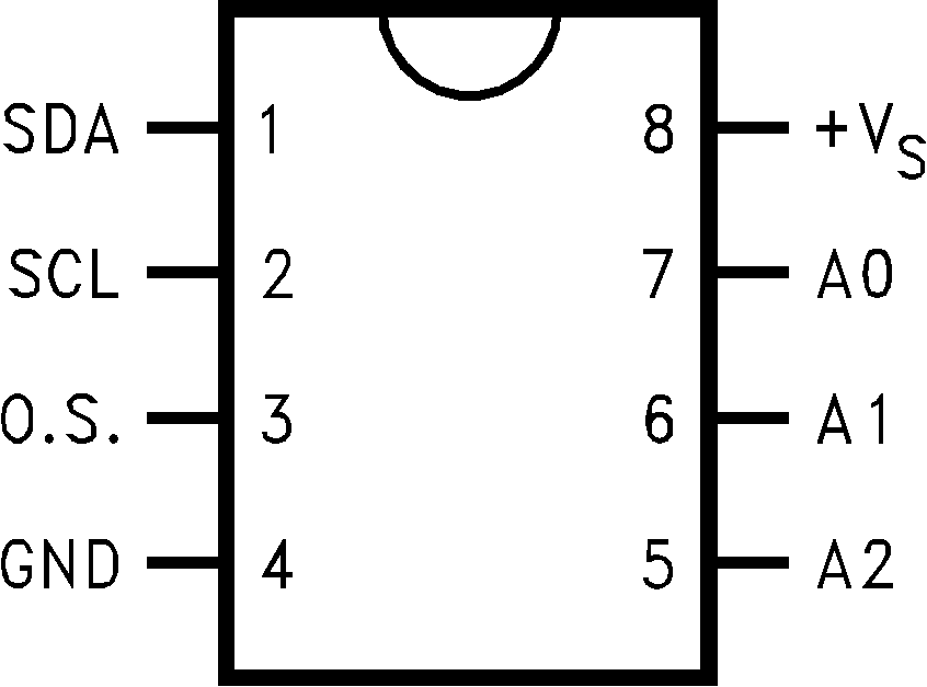
5 Pin Configuration and Functions

D and DGK Packages
8-Pin SOIC, VSSOP
Top View
LM75B LM75C 30099802.png

Pin Functions

PIN DESCRIPTION TYPICAL CONNECTION
NO. NAME
1 SDA I2C Serial Bi-Directional Data Line.
Open Drain.
From Controller, tied to a pullup resistor or current source
2 SCL I2C Clock Input From Controller, tied to a pullup resistor or current source
3 O.S. Over temperature Shutdown.
Open Drain Output
Pullup Resistor, Controller Interrupt Line
4 GND Power Supply Ground Ground
5 A2 User-Set I2C Address Inputs Ground (Low, 0) or +VS (High, 1)
6 A1
7 A0
8 +VS Positive Supply Voltage Input DC Voltage from 3 V to 5.5 V; 100-nF bypass capacitor with 10-µF bulk capacitance in the near vicinity