ZHCSE83A July 2015 – October 2015 LM74610-Q1
PRODUCTION DATA.
- 1 特性
- 2 应用
- 3 说明
- 4 修订历史记录
- 5 Pin Configuration and Functions
- 6 Specifications
- 7 Detailed Description
- 8 Application and Implementation
- 9 Power Supply Recommendations
- 10Layout
- 11器件和文档支持
- 12机械封装和可订购信息
7 Detailed Description
7.1 Overview
Most systems in automotive or industrial applications require fast response reverse polarity protection at the input stage. Schottky diodes or PFETs are typically used in most power systems to protect the load in case of negative polarity. The disadvantage of using diodes is high voltage drop during forward conduction, which reduces the available voltage and increases the associated power losses. PFET solutions are inefficient for high load current and low input voltage. These situations often occur during start-stop or cold crank. The other disadvantages of PFET include higher Iq and higher system cost. Using an N-Channel MOSFET with a controller IC can be a highly effective and more efficient substitute in reverse polarity protection circuitry. The ON state forward voltage loss in a MOSFET depends upon the RDSON of the MOSFET. The power losses become substantially lower than the Schottky diode for the equivalent current. This solution has a small increase in complexity; however it eliminates the need for diode heatsinks or a large thermal copper area in PCB layout for high power applications, that a diode would need.
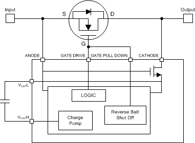
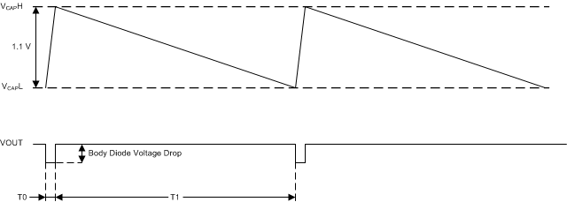
The LM74610-Q1 is a zero Iq controller that is combined with an external N-channel MOSFET to replace a diode or PFET reverse polarity solution in power systems. The voltage across the MOSFET source and drain is constantly monitored by the LM74610-Q1 Anode and Cathode pins. An internal charge pump is used to provide the GATE drive for the external MOSFET. The forward conduction is through the MOSFET 98% of the time. The forward conduction is through the MOSFET body diode for 2% of time when energy is stored in an external charge pump capacitor Vcap Figure 9. This stored energy is used to drive the gate of MOSFET. The voltage drop depends on the RDSONof a particular MOSFET in use, which is significantly smaller than a PFET. The LM74610-Q1 has no ground reference which makes it identical to a diode.
7.2 Functional Block Diagram

7.3 Feature Description
7.3.1 During T0
When power is initially applied, the load current (ID) will flow through the body diode of the MOSFET and produce a voltage drop (Vf) during T0 in Figure 8. This forward voltage drop (Vf) across the body diode of the MOSFET is used to charge up the charge pump capacitor Vcap. During this time, the charge pump capacitor Vcap is charged to a higher threshold of 6.3V (typical).
 Figure 8. Output Voltage and VGSOperation at 1A Output Current
7.3.2 During T1
Once the voltage on the capacitor reaches a higher voltage level of 6.3V (typical), the charge pump is disabled and the MOSFET turns ON. The energy stored in the capacitor is used to provide the gate drive for the MOSFET (T1 in Figure 8). When the MOSFET is ON, it provides a low resistive path for the drain current to flow and minimizes the power dissipation associated with forward conduction. The power losses during the MOSFET ON state depend primarily on the RDSON of the selected MOSFET and load current. At time when the capacitor voltage reaches its lower threshold VcapL 5.15V (typical), the MOSFET gate turns OFF. The drain current ID will then begin to flow through the body diode of the MOSFET, causing the MOSFET body diode voltage drop to appear across Anode and Cathode pins. The charge pump circuitry is re-activated and begins charging the Vcap. The LM74610-Q1 operation keeps the MOSFET ON at approximately 98% duty cycle (typical) regardless of the external charge pump capacitor value. This is the key factor to minimizing the power losses. The forward voltage drop during this time is limited by the RDSON of the MOSFET.
7.3.3 Pin Operation
7.3.3.1 Anode and Cathode Pins
The LM74610-Q1 Anode and Cathode pins are connected to the source and drain of the external MOSFET. The current into the Anode pin is 30 µA (typical). When power is initially applied, the load current flows through the body diode of the external MOSFET, the voltage across Anode and Cathode pins is equal to the forward diode drop (Vf). The minimum value of Vf required to enable the charge pump circuitry is 0.48V. Once the MOSFET is turned ON, the Anode and Cathode pins constantly sense the voltage difference across the MOSFET to determine the magnitude and polarity of the voltage across it. When the MOSFET is on, the voltage difference across Anode and Cathode pins depends on the RDSON and load current. If voltage difference across source and drain of the external MOSFET becomes negative, this is sensed as a fault condition by Anode and Cathode pins and gate is turned off by Gate Pull Down pin as shown in Figure 1. The reverse voltage threshold across Anode and Cathode to detect the fault condition is -20 mV. The consistent sensing of voltage polarity across the MOSFET enables the LM74610-Q1 to provide a fast response to the power source failure and limit the amount and duration of the reverse current flow.
7.3.3.2 VcapH and VcapL Pins
VcapH and VcapL are high and low voltage thresholds respectively that the LM74610-Q1 uses to detect when to turn the charge pump circuitry ON and OFF. The capacitor charging and discharging time can be correlated to the duty cycle of the MOSFET gate. Figure 9 shows the voltage behavior across the Vcap. During the time period T0, the capacitor is storing energy from the charge pump. The MOSFET is turned off and current flow is only through the body diode during this time period. The conduction though body diode of the MOSFET is for a very small period of time (2% typical) which rules out the chances of overheating the MOSFET, regardless of the output current. Once the capacitor voltage reaches its high threshold, the MOSFET is turned off and charge pump circuity is deactivated until the Vcap reaches its low voltage threshold (T1). The voltage difference between Vcap high and low threshold is typically 1.15V. The LM74610-Q1 charge pump has 46µA charging capability with 5-8MHz frequency.
 Figure 9. Vcap Charging and Discarding by the Charge Pump
The Vcap current consumption is 1 µA (typical) to drive the gate. The MOSFET OFF time (T0) and ON time (T1) can be calculated using the following expression

Where:
- C = Vcap Capacitance
- dV = 1.15V
- dI = 46 µA for charging
- dI = 0.95 µA for discharging
Note: Temperature dependence of these parameters – The duty cycle is dependent on temperature since the capacitance variation over temperature has a direct correlation to the MOSFET OFF and ON periods and the frequency. If the capacitor varies 20% the periods and the frequency will also vary by 20% so it is recommended to use a quality X7R/COG cap and not to place the cap in close proximity to high temperature devices. The variation of the capacitor does not have a thermal impact in the application as the duty cycle does not change.
7.3.3.3 Gate Drive Pin
When the charge pump capacitor is charged to the high voltage level of 6.3V (typ), the Gate Drive pin provides a 6.8µA (typ) of drive current. When the charge pump capacitor reaches its lower voltage threshold of 5.15V (typ), Gate is pulled down to the Anode voltage (Vin). When Anode voltage goes negative, the Gate voltage is pulled down to Anode voltage with 160mA pull down current.
7.3.3.4 Gate Pull Down Pin
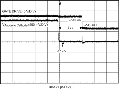
The Gate Pull Down pin is connected to the Gate Drive pin in a typical application circuit. When the controller detects negative polarity, possibly due to failure of the input supply or voltage ripple, the Pull-Down quickly discharges the MOSFET gate through a discharge transistor. This fast pull down react/s regardless of the Vcap charge level. If the input supply abruptly fails, as would happen if the supply gets shorted to ground, a reverse current will temporarily flow through the MOSFET. This reverse current can be due to parallel connected supplies and load capacitance and is dependent upon the RDSON of the MOSFET. When the negative voltage across the Anode and Cathode pins due to reverse current reaches -20mV (typical), the LM74610-Q1 immediately reacts and discharges the MOSFET gate capacitance as shown in Figure 10 . A MOSFET with 5nF of effective gate capacitance can be turned off by the LM74610-Q1 within 2µs (typical). The fast turnoff time minimizes the reverse current flow from MOSFET drain by opening the circuit. The reverse leakage current does not exceed 110µA for a constant 13.5V reverse voltage across Anode and Cathode pins. The reverse leakage current for a Schottky diode is 15mA under the same voltage and temperature conditions.
 Figure 10. Gate Pull Down in the Event of Reverse Polarity
7.4 Device Functional Modes
The LM74610-Q1 operates in two modes:
- Body Diode Conduction Mode
- The MOSFET Conduction Mode
The LM74610-Q1 solution works like a conventional diode during this time with higher forward voltage drop. The power dissipation during this time can be given as:

However, the current only flows through the body diode while the MOSFET gate is being charged to VGS(TH). This conduction is only for 2% duty cycle, therefore it does not cause any thermal issues.

The MOSFET is turned on during this time and current flow is only through the MOSFET. The forward voltage drop and power losses are limited by the RDSON of the specific MOSFET used in the solution. The LM74610-Q1 solution output is comprised of the MOSFET conduction mode for 98% of its duty cycle. This time period is given by the following expression:

7.4.1 Duty Cycle Calculation
The LM74610-Q1 has an operating duty cycle of 98% at 25 ̊C and >90% at 125 ̊C. The duty cycle doesn’t depend on the Vcap capacitance value. However, the variation in capacitance value over temperature has direct correlation to the switching frequency between the MOSFET and body diode. If the capacitance value decreases, the charging and discharging time will also decrease, causing more frequent switching between body diode and the MOSFET condition. The following expression can be used to calculate the duty cycle of the LM74610-Q1:
