ZHCSJI1A March   2019  – June 2019 LM66100

PRODUCTION DATA.  

  1. 特性
  2. 应用
  3. 说明
    1.     典型应用
  4. 修订历史记录
  5. Pin Configuration and Functions
    1.     Pin Functions
  6. Specifications
    1. 6.1 Absolute Maximum Ratings
    2. 6.2 ESD Ratings
    3. 6.3 Recommended Operating Conditions
    4. 6.4 Thermal Information
    5. 6.5 Electrical Characteristics
    6. 6.6 Switching Characteristics
    7. 6.7 Typical Characteristics
  7. Parameter Measurement Information
  8. Detailed Description
    1. 8.1 Overview
    2. 8.2 Functional Block Diagram
    3. 8.3 Feature Description
      1. 8.3.1 Reverse Polarity Protection (RPP)
      2. 8.3.2 Always-ON Reverse Current Blocking (RCB)
    4. 8.4 Device Functional Modes
  9. Application and Implementation
    1. 9.1 Application Information
    2. 9.2 Typical Applications
      1. 9.2.1 Dual Ideal Diode ORing
        1. 9.2.1.1 Design Requirements
        2. 9.2.1.2 Detailed Design Procedure
        3. 9.2.1.3 Application Curves
      2. 9.2.2 Dual Ideal Diode ORing for Continuous Output Power
        1. 9.2.2.1 Design Requirements
        2. 9.2.2.2 Application Curves
      3. 9.2.3 ORing with Discrete MOSFET
        1. 9.2.3.1 Design Requirements
        2. 9.2.3.2 Application Curves
  10. 10Power Supply Recommendations
  11. 11Layout
    1. 11.1 Layout Guidelines
    2. 11.2 Layout Example
  12. 12器件和文档支持
    1. 12.1 接收文档更新通知
    2. 12.2 社区资源
    3. 12.3 商标
    4. 12.4 静电放电警告
    5. 12.5 Glossary
  13. 13机械、封装和可订购信息

封装选项

机械数据 (封装 | 引脚)
散热焊盘机械数据 (封装 | 引脚)
订购信息

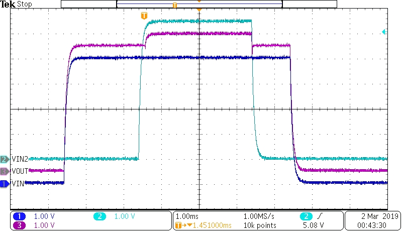
Application Curves

The below scope shot shows the output voltage (VOUT) being initially powered by VIN1. When VIN2 is applied, it powers VOUT because it is a higher voltage. When VIN2 is removed, VOUT is once again powered by VIN1.
LM66100 ORing_Scope.jpg
Figure 16. Dual Ideal Diode ORing Behavior