ZHCSN39A February 2020 – November 2021 LM61480 , LM61495 , LM62460
PRODUCTION DATA
- 1 特性
- 2 应用
- 3 说明
- 4 Revision History
- 5 Device Comparison Table
- 6 Pin Configuration and Functions
- 7 Specifications
-
8 Detailed Description
- 8.1 Overview
- 8.2 Functional Block Diagram
- 8.3
Feature Description
- 8.3.1 Output Voltage Selection
- 8.3.2 Enable EN Pin and Use as VIN UVLO
- 8.3.3 SYNC/MODE Uses for Synchronization
- 8.3.4 Clock Locking
- 8.3.5 Adjustable Switching Frequency
- 8.3.6 RESET Output Operation
- 8.3.7 Internal LDO, VCC UVLO, and BIAS Input
- 8.3.8 Bootstrap Voltage and VCBOOT-UVLO (CBOOT Pin)
- 8.3.9 Adjustable SW Node Slew Rate
- 8.3.10 Spread Spectrum
- 8.3.11 Soft Start and Recovery From Dropout
- 8.3.12 Overcurrent and Short Circuit Protection
- 8.3.13 Hiccup
- 8.3.14 Thermal Shutdown
- 8.4 Device Functional Modes
-
9 Application and Implementation
- 9.1 Application Information
- 9.2
Typical Application
- 9.2.1 Design Requirements
- 9.2.2
Detailed Design Procedure
- 9.2.2.1 Choosing the Switching Frequency
- 9.2.2.2 Setting the Output Voltage
- 9.2.2.3 Inductor Selection
- 9.2.2.4 Output Capacitor Selection
- 9.2.2.5 Input Capacitor Selection
- 9.2.2.6 BOOT Capacitor
- 9.2.2.7 BOOT Resistor
- 9.2.2.8 VCC
- 9.2.2.9 CFF and RFF Selection
- 9.2.2.10 RSPSP Selection
- 9.2.2.11 RT Selection
- 9.2.2.12 RMODE Selection
- 9.2.2.13 External UVLO
- 9.2.2.14 Maximum Ambient Temperature
- 9.2.3 Application Curves
- 10Power Supply Recommendations
- 11Layout
- 12Device and Documentation Support
- 13Mechanical, Packaging, and Orderable Information
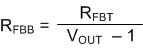
8.3.1 Output Voltage Selection
A voltage divider between output voltage and the FB pin is used to adjust output voltage. See Figure 8-1.
 Figure 8-1 Setting Output Voltage of Adjustable Versions
The LM6x4xx uses a 1-V reference for control to derive Equation 1. This equation can be used to determine RFBB for a desired output voltage and a given RFBT. Usually, RFBT is limited to a maximum value of 100 kΩ to prevent shifting due to PCB leakage under harsh conditions. A larger resistance of up to 1 MΩ can be used to improve light load efficiency in cleaner environments, or the fixed output voltage options under harsher conditions.
In addition, a feedforward capacitor CFF can be used to optimize the transient response.