ZHCSN39A February 2020 – November 2021 LM61480 , LM61495 , LM62460
PRODUCTION DATA
- 1 特性
- 2 应用
- 3 说明
- 4 Revision History
- 5 Device Comparison Table
- 6 Pin Configuration and Functions
- 7 Specifications
-
8 Detailed Description
- 8.1 Overview
- 8.2 Functional Block Diagram
- 8.3
Feature Description
- 8.3.1 Output Voltage Selection
- 8.3.2 Enable EN Pin and Use as VIN UVLO
- 8.3.3 SYNC/MODE Uses for Synchronization
- 8.3.4 Clock Locking
- 8.3.5 Adjustable Switching Frequency
- 8.3.6 RESET Output Operation
- 8.3.7 Internal LDO, VCC UVLO, and BIAS Input
- 8.3.8 Bootstrap Voltage and VCBOOT-UVLO (CBOOT Pin)
- 8.3.9 Adjustable SW Node Slew Rate
- 8.3.10 Spread Spectrum
- 8.3.11 Soft Start and Recovery From Dropout
- 8.3.12 Overcurrent and Short Circuit Protection
- 8.3.13 Hiccup
- 8.3.14 Thermal Shutdown
- 8.4 Device Functional Modes
-
9 Application and Implementation
- 9.1 Application Information
- 9.2
Typical Application
- 9.2.1 Design Requirements
- 9.2.2
Detailed Design Procedure
- 9.2.2.1 Choosing the Switching Frequency
- 9.2.2.2 Setting the Output Voltage
- 9.2.2.3 Inductor Selection
- 9.2.2.4 Output Capacitor Selection
- 9.2.2.5 Input Capacitor Selection
- 9.2.2.6 BOOT Capacitor
- 9.2.2.7 BOOT Resistor
- 9.2.2.8 VCC
- 9.2.2.9 CFF and RFF Selection
- 9.2.2.10 RSPSP Selection
- 9.2.2.11 RT Selection
- 9.2.2.12 RMODE Selection
- 9.2.2.13 External UVLO
- 9.2.2.14 Maximum Ambient Temperature
- 9.2.3 Application Curves
- 10Power Supply Recommendations
- 11Layout
- 12Device and Documentation Support
- 13Mechanical, Packaging, and Orderable Information
11.1 Layout Guidelines
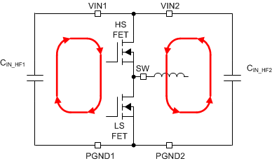
The PCB layout of any DC-DC converter is critical to the optimal performance of the design. Bad PCB layout can disrupt the operation of an otherwise good schematic design. Even if the converter regulates correctly, bad PCB layout can mean the difference between a robust design and one that cannot be mass produced. Furthermore, the EMI performance of the regulator is dependent on the PCB layout to a great extent. In a buck converter, the most EMI-critical PCB feature is the loop formed by the input capacitor or capacitors and power ground. This is shown in Figure 11-1. This loop carries large transient currents that can cause large transient voltages when reacting with the trace inductance. Excessive transient voltages can disrupt the proper operation of the converter. Because of this, the traces in this loop must be wide and short while keeping the loop area as small as possible to reduce the parasitic inductance. Figure 11-2 shows a recommended layout for the critical components of the LM6x4xx circuit.
- Place the input capacitor or capacitors as close as possible to the input pin pairs: VIN1 to PGND1 and VIN2 to PGND2. Place the small capacitors closest. Each pair of pins are adjacent, simplifying the input capacitor placement. With the QFN package, there are two VIN/PGND pairs on either side of the package. This provides a symmetrical layout and helps minimize switching noise and EMI generation. Use a wide VIN plane on a mid-layer to connect both of the VIN pairs together to the input supply. It is best to route symmetrically from the supply to each VIN pin to best utilize the benefits of the symmetric pinout.
- Place the bypass capacitor for VCC close to the VCC pin and AGND pin: This capacitor must be routed with short, wide traces to the VCC and AGND pins.
- Place the CBOOT capacitor as close as possible to the device with short, wide traces to the CBOOT and SW pins: It is important to route the SW connection under the device through the gap between VIN2 and RBOOT pins, reducing exposed SW node area. If an RBOOT resistor is used, place it as close as possible to the CBOOT and RBOOT pins. If high efficiency is desired, RBOOT and CBOOT pins can be shorted. This short must be placed as close as possible to the RBOOT and CBOOT pins.
- Place the feedback divider as close as possible to the FB pin of the device: Place RFBB, RFBT, CFF if used, and RFF if used, physically close to the device. The connections to FB and AGND through RFBB must be short and close to those pins on the device. The connection to VOUT can be somewhat longer. However, this latter trace must not be routed near any noise source (such as the SW node) that can capacitively couple into the feedback path of the regulator.
- Layer 2 of the PCB must be a ground plane: This plane acts as a noise shield and as a heat dissipation path. Using layer 2 reduces the inclosed area in the input circulating current in the input loop, reducing inductance.
- Provide wide paths for VIN, VOUT, and GND: These paths must be as wide and direct as possible to reduce any voltage drops on the input or output paths of the converter to maximize efficiency.
- Provide enough PCB area for proper heat sinking: Enough copper area must be used to ensure a low RθJA, considering maximum load current and ambient temperature. Make the top and bottom PCB layers with two-ounce copper and no less than one ounce. If the PCB design uses multiple copper layers (recommended), thermal vias can also be connected to the inner layer heat-spreading ground planes. Note that the package of this device dissipates heat through all pins. Wide traces can be used for all pins except where noise considerations dictate minimization of area.
- Keep switch area small: Keep the copper area connecting the SW pin to the inductor as short and wide as possible. At the same time, the total area of this node must be minimized to help reduce radiated EMI.
 Figure 11-1 Input Current Loop