ZHCSHU8F October 2008 – July 2019 LM5575-Q1
PRODUCTION DATA.
- 1 特性
- 2 应用
- 3 说明
- 4 修订历史记录
- 5 Pin Configuration and Functions
- 6 Specifications
- 7 Detailed Description
- 8 Application and Implementation
- 9 Power Supply Recommendations
- 10Layout
- 11器件和文档支持
- 12机械、封装和可订购信息
7.4.1 High-Voltage Start-Up Regulator
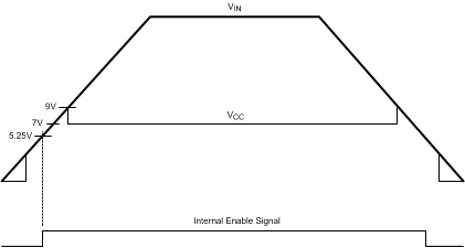
The LM5575-Q1 contains a dual-mode internal high-voltage start-up regulator that provides the VCC bias supply for the PWM controller and bootstrap MOSFET gate driver. The input pin (VIN) can be connected directly to the input voltage, as high as 75 V. For input voltages lower than 9 V, a low dropout switch connects VCC directly to VIN. In this supply range, VCC is approximately equal to VIN. For VIN voltage greater than 9 V, the low-dropout switch is disabled and the VCC regulator is enabled to maintain VCC at approximately 7 V. The wide operating range of 6 V to 75 V is achieved through the use of this dual-mode regulator.
The output of the VCC regulator is current-limited to 25 mA. Upon power up, the regulator sources current into the capacitor connected to the VCC pin. When the voltage at the VCC pin exceeds the VCC UVLO threshold of 5.35 V and the SD pin is greater than 1.225 V, the output switch is enabled and a soft-start sequence begins. The output switch remains enabled until VCC falls below 5 V or the SD pin falls below 1.125 V.
An auxiliary supply voltage can be applied to the VCC pin to reduce the IC power dissipation. If the auxiliary voltage is greater than 7.3 V, the internal regulator essentially shuts off, reducing the IC power dissipation. The VCC regulator series pass transistor includes a diode between VCC and VIN that should not be forward biased in normal operation. Therefore the auxiliary VCC voltage should never exceed the VIN voltage.
In high-voltage applications, take care to ensure the VIN pin does not exceed the absolute maximum voltage rating of 76 V. During line or load transients, voltage ringing on the VIN line that exceeds the absolute maximum ratings can damage the IC. Both careful printed-circuit board layout and the use of quality bypass capacitors located close to the VIN and GND pins are essential.
 Figure 8. VIN and VCC Sequencing